
What are the Problems that need to be avoided In PCB Assembly Process?


PCBs are an integral component of any electronic device be it a small toy or a sophisticated computer. Its complex interconnected components comprising of resistors, diodes, capacitors and more allow the device to work in tandem. In a sense it is like the “brain” of the system”. In high reliability systems particularly — such as oilrigs, space satellites and others failures can have devastating consequences. It is critical, therefore the PCB Assembly process is flawless and common mistakes in the assembly are watched out for.
Here are some of the factors to watch out for PCB Problem and solution:
Supply Chain Management
To be able to create high quality PCBs, the one thing that needs to be in order is the supply chain. It is important to check their availability, quality as well as price. Consistent ability to source the components is critical towards managing the manufacturing cycle of the product. You also need to be doubly sure of the quality of the products. Counterfeit components can have disastrous consequences on the product performance and your reputation. It is also important to check the lead-time of components especially as the volumes required increase. While you may take initial samples directly from manufacturers, remember to budget for lead times as volumes go up.
PCB layout
A common problem faced at the manufacturing stage is the nuances in PCB layout. While several designs may look good on paper, manufacturing them may be a different ball game. For example if the design has a large number of components positioned closely together, soldering them may be an issue. In case of a double-sided PCB, you need to make sure that the largest components are placed on one side. Essentially you need to make sure that the pcb layout is indeed viable at the manufacturing stage. If for example, holding down complicated parts requires them to be glued manually, it will add to your assembly time as also leave margins of error.
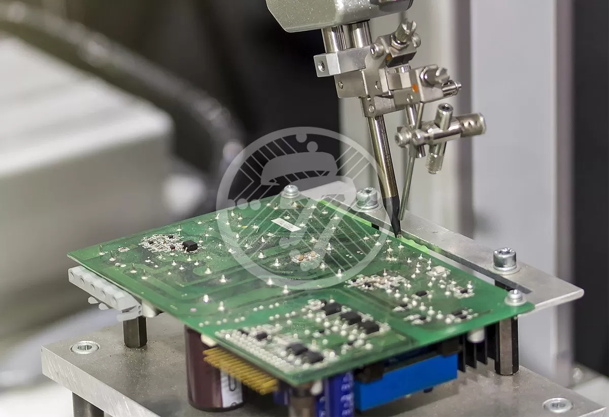
PCB Testing
A common problem associated with PCB Assembly, is that the testing is often done after the manufacturing. What needs to be done, however, is to design the test points as you conceive the design. There are in fact a whole lot of PCB Functional testing ensure that the PCB is functioning correctly.
Some of PCB tests include:
- Micro-sectioning Analysis- Also referred to as Cross sectioning, this test helps to identify component defects as also a thermo mechanical failures.
- Solderability Testing- This test helps test PCB pad solderability to ensure that the surface is robust so that the solder joint will be reliable. It also helps to determine if storage will lead to any effects on the solder components.
- PCB Contamination Testing- This tests a number of issues such as corrosion and degradation. Very often handling, flux residues etc can lead to contamination which can in turn lead to part failure. The contamination analysis is known for its accuracy and precision.
- Optical Microscopy- This tests the PCB for problems associated with soldering and overall assembly. The process is known for its speed as it involves using a high power microscope to check for improper construction.
- X-ray Inspection- A Non-invasive test, this lays bare any surface and internal defects with ease.
A whole lot of PCB Challenges also emanate from the fact that increasingly components are shrinking in size and circuits are becoming more and more sophisticated. Therefore, all the more chances of defects in the assembly.
The challenges faced by failure analysts are therefore many, printed circuit board common problems such as:
- Growing popularity of High-speed Printed Circuit Boards (HSPCBs) – These require boards that are made up of two or three materials that increase the chances of failure. Added to this is the fact that it requires pins and chip placed in a correct manner.
- Lead-free Assembly Process- This requires high temperature and a traditional tin solder.
- Hole Barrel Cracking- A lot of the failure happens on account of barrel fatigue because of the differential expansion of the copper plating and the printed board.
- Conductive Anodic Filament- This is an electro chemical process that can cause leakage and a breakdown between conductors.
PCB Assembly therefore requires an effective root cause analysis to ensure that corrective action is taken so that the problem does not recur. In addition a detailed failure analysis ensures ways to improve the product as also to correct faults that may not have been noticed at the design stage.
Technotronix offers professional PCB Assembly services with 40 years of expertise. Our accurate PCB assembly process meets the quality standards, including ISO-9001:2015, RoHS, and more. You can rely on our PCB design tools that, in turn, lead to that perfect PCB Assembly. Our superior engineering capabilities mean that each board matches your exact requirements and technical specifications. If you have any questions or any requirements related to PCB assembly service, please feel free to contact us via email at sales@technotronix.us or call at 714/630-9200.
Get a free Quote for PCB Assembly Services!