
Design for Manufacturability (DFM) is an approach to product design that emphasizes optimizing the design for ease of manufacturing. It involves considering manufacturability factors such as material selection, component placement, assembly processes, and production constraints early in the design phase. The goal of DFM is to simplify manufacturing operations, reduce production costs, minimize assembly time, and enhance product quality and reliability. By implementing DFM principles, designers and engineers ensure that the final product can be efficiently and economically manufactured without compromising its functionality or performance.
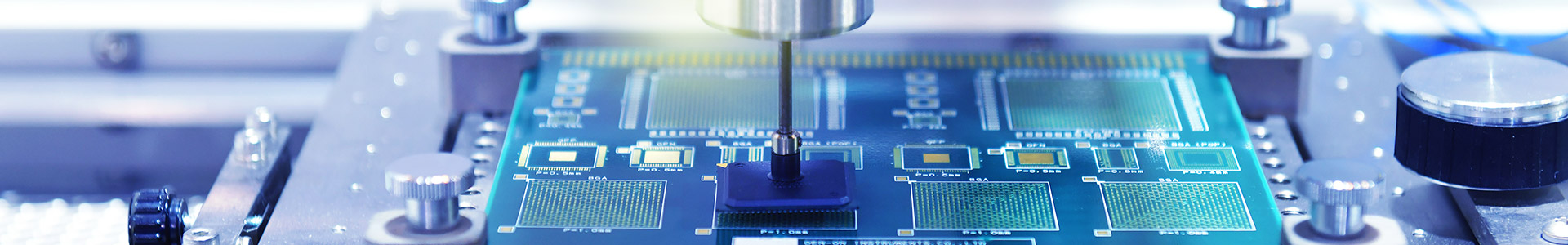
Design For Manufacturability
With new electronic designs vying for consumer attention every day, it is crucial to not only have outstanding designs but also those that can be built quickly, efficiently, and at the lowest manufacturing costs. This is the core function of design for manufacturability (DFM). Simply put, DFM and design for assembly (DFA) optimize a prototype before manufacture. The goal is to determine how to design a product so that it can be manufactured and assembled cost-effectively.
DFM focuses on reducing the overall manufacturing cost, while DFA aims to reduce material usage, capital overhead costs, and labor. Both approaches apply necessary standards to minimize product development cycle time and prevent costly errors later.
In PCB DFM, printed circuit board manufacturers in the USA ensure that designs are optimized for efficient production, maintaining high quality and reliability. By integrating DFM and DFA principles, manufacturers can produce superior products quickly and cost-effectively. This ensures a seamless transition from design to production, ultimately delivering high-performance electronic products to the market with reduced development times and lower costs.
Some of the rules that PCB design for manufacturing as well as design for assembly strive towards, include:
- Reducing the number of parts in a design.
- Using multifunctional components.
- Designing for ease of PCB fabrication.
- Maximization of component placement acceptance.
- Minimizing repositioning and handling during assembly.
At Technotronix, we are fully equipped with the technological know-how, an experienced team and industry best practices that enable us to carry out the necessary design for manufacturing tests that ensure manufacturing of a superior product.

PCB Design for Manufacturability
Our DFM capabilities span the following areas:

Manufacturing Process
With our expertise, we determine the right manufacturing processes for the PCB. The considerations at this stage include:
- Dimensions
- Size
- Material required
- Tolerance
- Steps required in assembly, and more.
- Functionality

Product Design
This part of the design for manufacturability exercise involves rectifying any design issues prior to manufacturing. All design modifications are made keeping into account fundamental design principles.

Product Material
This involves determining what materials are necessary for production. This step involves checking for strength, texture and thermal properties of the material.

Operating Environment
We undertake a thorough evaluation of the exact environment under which the product needs to operate. The impact of the environment on the material and shape of the product, for example, is determined at this stage.

Testing
The final stage is to determine whether the design and the materials used conform to the regulatory rules and standards set for the PCB.
The process and method of design for manufacturability
- PCB design for manufacturability (DFM) specifications are provided in detailed documents.
- Design for manufacturability checklists are prepared according to these specification documents during the product design planning phase.
- PCB DFM reports are then created to outline potential manufacturing issues.
- PCB design for manufacturability testing is conducted to ensure the design meets all manufacturability criteria.
- DFM analysis and evaluation are derived from the testing results to identify areas for improvement.
Incorporating DFM design for manufacturability and design for manufacturability and assembly principles ensures that the product is optimized for efficient and cost-effective production. By following these steps, manufacturers can minimize errors, reduce development time, and lower production costs, resulting in high-quality, reliable PCB products.
Benefits of PCB Design for Manufacturing
The benefits of PCB design for manufacturing are wide ranging. Broadly they include:
- Reduction of bill of material costs by optimizing component selection and placement.
- Decrease in handling costs through streamlined manufacturing processes.
- Lower labor and energy costs due to efficient assembly techniques.
- Shortened manufacturing time and enhanced efficiency in production lines.
- Enhanced product reliability through improved design and assembly practices.
- Increased profit margins by minimizing waste and maximizing yield.
Implementing PCB design for manufacturability (DFM) principles ensures these benefits are realized, optimizing every stage of the manufacturing process for cost-effectiveness and quality improvement. This approach not only enhances operational efficiency but also contributes to producing more reliable and competitive electronic products in the market.
Applications of Design for Manufacturability
Some examples of DFM tasks include:
- Comparing designs to see which one has the least manufacturability issues and the least cost.
- Identifying the design features that add to manufacturing operations.
- Ensuring that there are no design issues at the time of roll out that can turn out to be costly.
Technotronix Advantage
At Technotronix, we boast over 40 years of expertise in fabricating and assembling a diverse range of PCBs, including rigid, flex, and rigid-flex configurations. Our advanced equipment and skilled team are fully equipped to handle any PCB design for manufacturability challenge. Partnering with us grants you access to industry-leading practices that provide a competitive edge.
We utilize sophisticated manufacturing simulation tools for comprehensive DFM modeling, significantly reducing production time and costs. This capability is crucial for achieving quick time-to-market advantages in today's fast-paced industry landscape.
Committed to excellence, we offer rapid PCB design for manufacturability services without compromising on quality. Simply reach out to our team with your specific requirements, and our experienced professionals will provide a tailored quote and ensure precise fabrication to meet your exact specifications.
As one of the top printed circuit board manufacturers in the USA, we prioritize cost-effectiveness while delivering exceptional quality. Our streamlined processes and dedication to DFM ensure that your project remains competitive and meets the highest standards of reliability and performance in the market. Partner with Technotronix for reliable circuit board manufacturing services that exceed expectations.
PCB Design for Manufacturability FAQs
- Issues due to acid traps.
- Issues due to copper/solder mask slivers on planes.
- Used due to starved thermals.
- Issues due to no clearance pads on planes.
- Issues due to insufficient annular rings.
- Issues caused by copper being too close to the board edge.
Do you have any design for manufacturability requirements? Request a free design for manufacturability quote. Alternatively, email BoM, Gerber files, and other required details at sales@technotronix.us or call us 714/630-9200.

PCB Assembled in 24 hours
Kitted and Turn-Key option as per customers requirement.

REQUEST OUR BROCHURE
 Request Brochure
 Please provide your email address. We’ll send you copy of our brochure in a PDF format.