PCB Fabrication
Technotronix is an elite provider of custom PCB fabrication services with its multifaceted group of experts and ample experience in rendering electronics manufacturing services as our competency can be evidenced through our global customer base. Our guaranteed full fledge PCB fabrication services from product layout, manufacturing to warehousing & shipping have made it possible to have a top-notch customer retention ratio.
Our printed circuit board fabrication services are available in high volume, low volume printed circuit boards, full turnkey printed circuit boards, consignment PCB fab and more.
Technotronix has adopted advanced methods and latest technologies of PCB fabrication, which can ensure about the performance of fabricated printed circuit boards. Our experts are capable of managing every complex requirement of PCB fab services. We understand every need of our client and offer multilayer PCBs, quick turn PCB fab, rigid flex PCBs, RF circuit boards, ATE printed circuit boards, metal core PCB fabrication, standard PCB fabrication, custom PCB fabrication, hybrid PCB fab, PCB testing, and more.
Our capabilities have expanded in providing quick-turn PCB fabrication, NPI prototyping & fab, and multi-layer PCB fabrication to our customers when they want to introduce products to the market and require larger quantities in a short period of time.
Technotronix has its own state-of-art unit and PCB fabrication facilities in USA, where we offer standard printed circuit board fabrication services to our clients. Our experts are capable to manage everything from simple PCB layout to complex PCB design and single layer to multilayer PCB fabrication.
PCB Fabrication Services
We are working successfully for our customers in varied industries like aerospace, telecommunication, defense, medical, automotive, renewable energy, robotics and more. We have developed a personalized approach at every stage of the PCB Fabrication.
Multilayer PCB
Quick Turn PCB Fabrication
Prototype PCB Fabrication
LED Circuit Boards
High Frequency PCBs
Rogers PCB
High Temperature PCB
Metal Core PCB
RoHS Circuit Boards
Bare Board PCB
Rigid Flex PCBS
Flexible Circuit Boards
Rigid Printed Circuit Boards
Rapid Printed Circuit Board Prototype
RF Printed Circuit Boards
PCB Functional Testing
PCB Electrical Testing
ATE Printed Circuit Board
Standard PCB
Heavy Copper PCB
Hybrid PCB
CAPABILITIES OF PCB FABRICATION
We understand that different industries demand special fabricated PCBs. Meet your any kind of printed circuit board fabrication requirements with our capabilities:
- Shapes:
- Circular
- Rectangular
- Custom
- Circuit board base materials:
- RoHS compliant
- RF and advanced RF
- Aluminum clad
- Boards type:
- Metalcore
- Aluminum backed
- Rigid, flex, etc.
- Multilayer PCB up to 24 Layers
- Alternative finishes:
- Hot Air Solder Level
- Electroless Nickel / Immersion Gold
- Silver
- Electroless Tin Lead
- Organic ( OSP )
- Hard Gold ( edge contact )
- Carbon
- Peelable
- Designs:
- Countersinks and bores
- Controlled dielectric and impedance
- Cover coat
- Edge mill and Back drilling
- Drill:
- Small size
- Large size
- Control depth and positional tolerance
- Circuit boards parameters:
- Layer count and board thickness
- Copper weight
- Printed Circuit Board Profiling:
- CNC Rout
- CNC Score
- Pierce Blank & Return
- Advanced options:
- Carbon mask
- Golf fingers and edge plating
- Kapton tape
- Advance designs:
- Blind Vias
- Buried Vias
- Multilayer design
- Stacked micro vias
- Certifications:
- Certified for military
- Certified for aerospace
- Certified for other applications, etc.
- Bare Board Test:
- Bed of Nails
- Simultaneous double-sided flying probe test
Benefits of PCB Fabrication
Quality control
We have implemented ISO 9001:2015 and ISO 13485:2016 quality management system to provide our customer the best quality PCB fab service.
Expected Cost
Overall cost is dependent on the complexity of the device. Mostly, PCB fabrication time, amount of materials, labor work, and required energy is calculated for the cost. So, you can easily analyze the cost.
Quick Turnaround Time
We offer quick turnaround times that significantly impact your go-to-market plans. In addition, our overall culture of customer centricity and responsiveness ensures that you get quick quotes and support.
Security and Safety
We consider security and safety concern of industry and carried out the solution for PCB fabrication and PCB assembly process phases based on industrial standards and guidelines!
Classification of PCB Fabrication
Fabrication of printed circuit boards (Fabrication of PCB) is done in several ways. These are classified as:
- PCB Milling: It is also known as the isolation milling, which refers the process of removing areas of copper from a sheet of PCB materials.
- Etched circuit boards: It usually removes unwanted copper by using acid to produce the well-printed circuit boards.
- Toner transfer method: You can make a printed circuit board very quickly by using this method. You can print the circuit by using a laser printer.
- Perforated plates and experimental plates: It is more stable compared to other plates. It contains a few holes that give high resistance.
PCB Fabrication process and technology
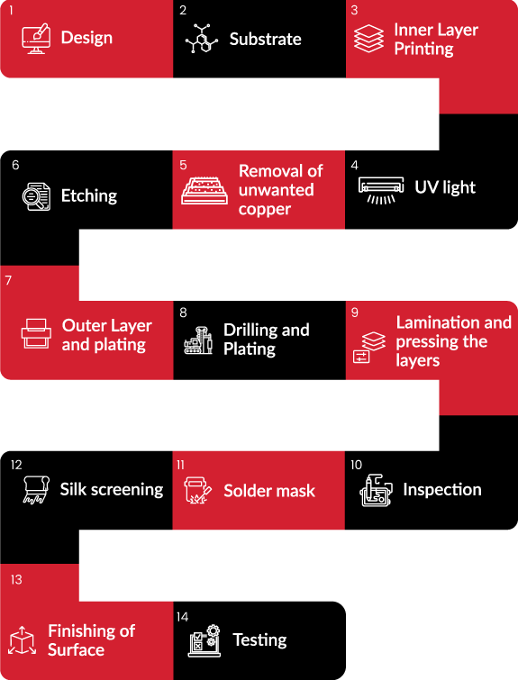
The complete PCB fabrication process is based on the design package that makes the circuit board in physical form. Following is the process of fabrication of PCB which starts with design and ends with testing:
Making Design and printing the Design
Make the Design of the board for the further process. Used it as a blueprint of your PCB. Various software is available for this; when the Design is ready, print it using a plotted printer.
Substrate
Create the substrate and make sure its material is insulated. Copper covers both sides of the layer.
Inner layer printing
Make sure the blueprint and real print are aligned. Hole the circuit board so that the whole Design is printed serially using photo-reactive chemicals
UV Light
It shows all the paths of copper. It hardens the photoresist. To remove additional photoresist, dip the circuit board in the chemical solution of alkaline.
Removal of unwanted copper
Dip the board in another solution, same as alkaline, to remove the extra copper. The photoresist stays. There is no side effect on the photoresist by using the chemicals.
Inspection
Now check that the layers are aligned or not by seeing the holes of the layers. After this step, you cannot rectify the mistakes of the previous steps. So do it carefully.
Laminating and pressing the layers
In this process, metals hold the layers because there is a fusion between the layers. Now, there is no requirement for a copper layer. Then press all the layers by using a mechanical press. Pin the layers so that they are aligned together.
Drilling and Plating
If any copper remains on the layers' inner surface, it is removed by drilling guided by the computer. A chemical solution fuses all the layers. Now you can plate the circuit board by fusing the layers using chemicals.
Outer layer and Plating
The outer layer of photoresist in the board is hardened by UV rays and removes the extra photoresist. Now the board is plated by a thin layer of copper. This acts as a guard of copper to protect it from etching.
Etching
Some chemical solution removes extra copper. Plating protects the required copper from the chemicals.
Solder mask
Clean the board before doing the solder mask. Commonly, the green part in the circuit board is a solder mask. UV rays can remove extra solder masks, and the required solder masks can be placed on the circuit board.
Silk screening
Important information is printed on the board by this process. After that, the last coating is needed on the board.
Finishing of Surface
According to the requirements, soldering is further processed to give good quality of PCB. It upgrades the standards of the boards.
Testing
Electrical tests are mandatory to complete the process. An expert technician does this to test the overall quality. It is necessary to check that the boards are working appropriately or not.
Why choose Technotronix as your PCB Fabrication provider?
We are known as the leading PCB fabrication service provider in California, USA. Our aim is to fulfil the demands of our customer base for PCB fabrication service. We are concerned about your every necessity. We have over 40 years of experience in providing printed circuit board fabrication services. We provide you products at an affordable price, including testing services. Feel free to ask if you have any questions regarding printed circuit board fabrication services. Your satisfaction is our priority.
PCB Fabrication FAQs

Looking for PCB fabrication service? You can use PCB Fabrication quote request form and submit information. Alternatively, you can email us BOM and Gerber files along with information of PCB Fabrication volume and type of PCB Fabrication testing requirements you might have on sales@technotronix.us or call us on 714/630-9200 in case any other clarification is required in respect to our PCB Fabrication services.
PCB Assembled in 24 hours
Kitted and Turn-Key option as per customers requirement.
REQUEST OUR BROCHURE
Please provide your email address. We’ll send you copy of our brochure in a PDF format.