Get Expert RF PCB services!
From prototype to volume, get manufacturing that meets your exact specifications. Reach out sales@technotronix.us.
Request a free quote!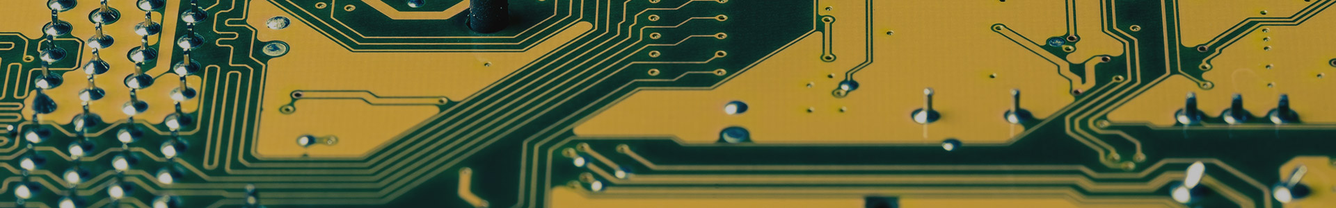
Engineered for high-frequency signal performance, we manufacture custom radio frequency printed circuit boards to deliver stability, and reliable signal integrity in demanding electronic applications. The manufacturing approach focuses on advanced materials, controlled impedance, and tightly regulated fabrication processes to support industries such as telecommunications, automotive, computer networking systems, aerospace, medical devices, wireless technologies, IoT devices, smartphones, sensors, robotics, and security. As an ISO 9001:2015 & AS9100 Rev. D Certified Company, we deliver RF board assemblies which are carefully evaluated to minimize signal loss, reduce interference, and maintain consistent performance under varying operating conditions.
| Features | Capabilities |
|---|---|
| Layer Count | 2-44 layers |
| Drill aspect ratio | 15:1 |
| Maximum Panel Size | 24″ x 30″ |
| Vias | Blind / Buried Vias. & Micro Vias Via In Pad with Fill Options (Conductive, Non-Conductive, Copper Plug) |
| Characteristic impedance of a transmission line | Controlled impedance |
| Minimum track and gaps | 0.75mm / 0.075 mm |
| Metal Core thickness | 58mm * 1010mm |
| Surface finish | HASL (Lead-free), OSP, ENIg, immersion tin, immersion silver. |
From prototype to volume, get manufacturing that meets your exact specifications. Reach out sales@technotronix.us.
Request a free quote! Request Brochure
 Please provide your email address. We’ll send you copy of our brochure in a PDF format.