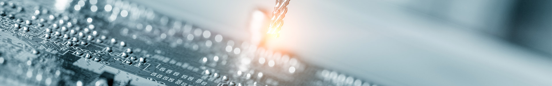
PCB Fabrication Process

pcb fabrication capabilities california

When it comes to creating a robust electronic product, the one thing that is extremely important, is to choose the right PCB assembly fabrication solution. On the other hand, lack of attention to the quality of your boards can result in costly mistakes, product failures and even lack of company reputation.

To be able to gauge the full import of this, it will be important to learn what really does Printed Circuit Board Fabrication involve and what is its importance in PCB development.

What does PCB Fabrication Process mean?

Even before defining circuit board fabrication, let us look at some of the other terms that are commonly associated with the PCB development process and understand the interrelationships between them.

Printed Circuit Board Fabrication

PCB Development

First up, let us look at the term PCB development. This is really the process of developing the PCB from the design stage to the production stage. Essentially this involves the processes of:

  • Design
  • Manufacturing
  • Testing
PCB Fabrication Capabilities

PCB Manufacturing

The other term commonly used is PCB manufacturing. This really is a two-step process comprising of:

  • Fabrication of PCB
  • PCB Assembly
PCB Development

PCB Testing

A crucial step post PCB Manufacturing, this is required to ensure that any errors are identified and changes required can be made so that there is no issue faced at a later date.

PCB Manufacturing

PCB Assembly

This step involves mounting the components on the bare board. This could be through a process of through hole or surface mount technology or even by way of a mix between the two.

The PCB Fabrication Process

With these terms clarified, let us move to the PCB Fabrication process. This is the process where the PCB design is converted into the physical structure. PCB Fabrication involves the following:

  • Imaging the layout on the copper clad laminates
  • The next step is to etch the excess copper
  • Laminating board materials and creating PCB layer stackup
  • Drilling holes
  • Etching of copper, this time from the surface layers
  • Plating pin holes and via holes
  • Solder masking
  • Silkscreen printing reference
  • Adding the requisite finish

There are also a number of printed circuit board fabrication methods, primary among them being:

  • Etching- This is known to be easy and cost-effective as it uses chemical solutions to remove unwanted areas from the board.
  • Manual- In this method a manual design is drawn onto the board.
  • Photographic- In this method, a drawing made of photoresist material is projected onto the board.
  • Direct etch- Here a design is printed on a laser printer. This is in turn ironed on to the circuit board.
  • Silkscreen- This involves the use of photosensitive material.
PCB Testing

It is extremely important to understand the PCB Fabrication process as it is an outsourced activity that a Contract Manufacturer performs for you as per the specifications provided by you. In many cases the contract manufacturer does not have access to the intent behind your design as well as the choice of material, layout etc. that is made by you. All of this, in turn, impacts the following:

Manufacturability - Simply put this follows from your design choices. For example, at the design stage you need to ensure that there are enough clearances between surface elements, the material selected has high Coefficient of thermal expansion, and more.

Yield Rate - If you specify parameters that stretch the tolerance of the equipment, you could land up in a situation where a large number of boards are not usable.

Reliability - It is important that your board’s construction meets the specified levels of reliability. For rigid boards, for example, there are 3 classification levels set. If the board does not meet the level of reliability desired, it could lead to inconsistencies in operation and even failure.

We endeavor to deliver following PCB Fabrication capabilities & core competences:

  • New Production Introduction (NPI)
  • High Mix Low Volume Circuit Board Production
  • Mass Production (High volume Low Mix)
  • Placement capability for package components
  • Package on Package (PoP)
  • Flying Probe and In Circuit testing
  • Thru Hole Technology – Selective Soldering/Wave Soldering
  • Box Build and System assembly
  • Coating/Potting
  • Final Packaging and Out of the Box experience
  • Multilayer PCB
  • Quick Turn PCB Fabrication
  • Prototype PCB Fabrication
  • LED Circuit Boards
  • High Frequency PCBs
  • Rogers PCB
  • High Temperature PCB
  • Metal Core PCB
  • RoHS Circuit Boards
  • Bare Board Printed Circuit Boards
  • Rigid Flex PCBs
  • Flexible Circuit Boards
  • Rigid Printed Circuit Boards
  • Rapid Printed Circuit Board Prototype
  • RF Printed Circuit Boards

With detailed knowledge about the PCB Fabrication process and PCB fab capabilities of the manufacturer, you will be able to make your design choices with caution as these choices will have far-reaching consequences in PCB development and production. It is imperative that the Design for Manufacturing guidelines be followed so as to ensure that you do not run into any problems at a later stage. This will also ensure that any delays as well as any unforeseen costs are avoided.

contact icon

Do you have any PCB Fabrication Capabilities requirements? Request a free PCB Fabrication quote. Alternatively, email BoM, Gerber files, and other required details at sales@technotronix.us or call us 714/630-9200.

Timer

PCB Assembled in 24 hours

Best Turn around time for Prototype PCB assembly.
Kitted and Turn-Key option as per customers requirement.
Timer

REQUEST OUR BROCHURE

To know more about Technotronix
Download Brochure Request Brochure
Request Brochure

Please provide your email address. We’ll send you copy of our brochure in a PDF format.

You have reached the end of a page.
Back to top