At Technotronix, our PCB Prototype solutions are designed to support fast, reliable, and cost-effective
product
development with quick-turn capabilities, including delivery in as little as 24 hours.
From Printed Circuit Board Prototype builds to complex multilayer boards, we provide quality
manufacturing, design
verification, and flexible assembly options to help engineers identify design issues early, reduce
production risks,
minimize costly revisions, and accelerate product development.
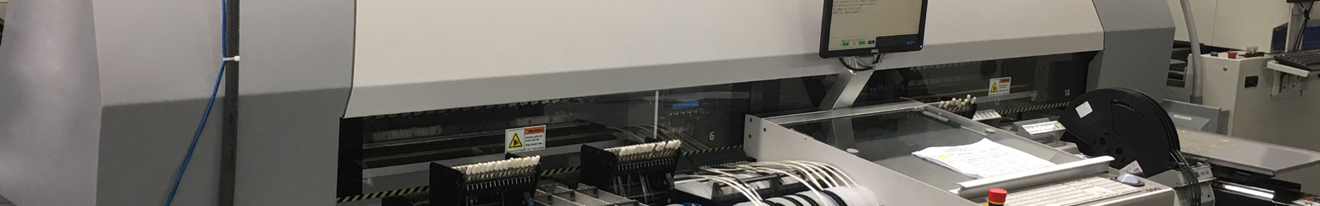
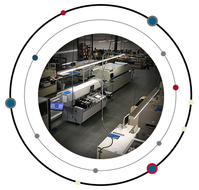
As an experienced PCB Prototype Manufacturer, we provide comprehensive PCB Prototyping Services using
advanced
manufacturing technologies, automated layout analysis, multilayer quick-turn fabrication, Surface Mount
Technology
(SMT), Chip-on-Board (COB), and Custom PCB Prototype solutions built from Gerber files and Bill of
Materials (BOM).
As a customer-focused PCB Prototyping Company, we prioritize project requirements, manufacturing quality,
and delivery
schedules to help customers move efficiently from concept to production.