Why does selecting a single PCB manufacturer for prototyping and mass production save time and costs?


Choosing one PCB (Printed Circuit Board) manufacturer for both prototyping and mass production is a practical strategy that benefits businesses of all sizes. It helps save time, reduce costs, and improve product quality. In today’s fast-moving electronics market, companies need to bring products to market quickly while keeping expenses under control. Working with a single manufacturer throughout the product life cycle is one of the best ways to meet these goals. In this article, we’ll break down why it’s smart to partner with a single PCB manufacturer. We’ll look at how this approach improves efficiency, communication, quality, and customer support.
Streamlined Communication and Collaboration
When you choose one manufacturer for both prototyping and production, communication becomes easier. The same team that handles your prototype will also be in charge of the full run. This leads to a better understanding of your design and fewer errors in translation.
Design feedback is faster, and your team gets consistent support throughout the process. You avoid delays that often happen when switching between vendors.
Consistent Quality and Standards
Using the same facility ensures that quality control methods remain consistent. You won’t have to worry about unexpected changes in material, process, or assembly between the prototype and production stages.
A single manufacturer understands your quality expectations from the start. They can carry this forward throughout the life of the project, helping reduce rework and quality issues.
Cost efficiency with bulk and repeat orders
A long-term partnership can lead to cost benefits. When you work with one vendor, you may get volume discounts, fewer shipping fees, and reduced setup charges.
Your manufacturer may also be able to stock components and materials for you, further cutting costs on future production runs.
Faster lead times from start to finish
Time is money, especially in competitive industries. When one vendor handles everything, they can move quickly from prototype to full-scale production. They don’t need to re-learn the design or manufacturing process.
You’ll see shorter lead times, quicker testing, and faster product launches.
Simplified Supply Chain
Dealing with multiple vendors adds complexity to your supply chain. Working with just one manufacturer makes supply chain management easier. This reduces risks and delays.
You only need to manage one point of contact, which simplifies tracking, logistics, and payments.
Fewer Errors and Smoother Revisions
A single manufacturer already knows your product and history. If design changes are needed, they can adjust quickly and accurately.
This avoids miscommunication and lowers the chance of errors that often happen when moving between vendors.
Better Customer Service and Support
When you build a strong relationship with your manufacturer, you get better support. They are more familiar with your needs and can respond to issues quickly.
You’ll also get more helpful advice on how to improve your designs or reduce costs over time.
Greater Traceability and Documentation
Using one manufacturer ensures consistent documentation. From prototypes to final products, your project history is in one place.
This helps with troubleshooting, product improvements, and compliance with industry standards.
Reduced Time to Market
A single PCB partner already has design files, build history, and process guidelines. That means fewer setup steps and less back-and-forth communication.
This saves valuable time during design revisions, approvals, and manufacturing ramp-up.
Improved long-term planning and scaling
A long-term manufacturing partner can scale with you. As your business grows, they can adjust production volumes and offer additional services.
This flexibility supports your business at every stage—from startup to full-scale operation.
Benefits of using the same PCB manufacturer for prototyping and production
When you choose the same manufacturer for all stages of PCB development, you avoid compatibility problems. The transition is smoother, and the manufacturer can fine-tune your design with real production insight.
This improves product reliability and helps avoid delays due to unexpected manufacturing issues.
Cost Savings in PCB Manufacturing with One Vendor
There are many hidden costs in working with multiple vendors: setup fees, shipping, onboarding, and even time lost to coordination. Working with one manufacturer eliminates many of these.
The result is better cost control and fewer surprises in your project budget.
Time Efficiency in PCB Prototyping and Production
Fast turnaround is key to staying ahead. With one manufacturing partner, you get quicker quotes, faster revisions, and shorter feedback loops.
That can make a big difference when time-to-market is critical.
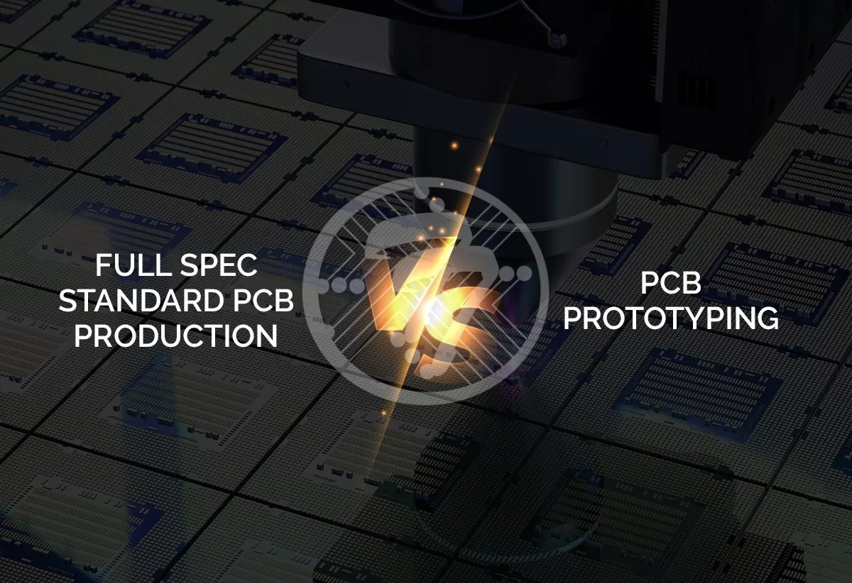
Seamless Transition from PCB Prototype to Full Production
Switching vendors often leads to delays. Design files might need re-formatting. Tooling may not match. Test procedures may differ.
When you stay with one vendor, none of these are issues. Your project flows smoothly from start to finish.
How to reduce lead times in PCB manufacturing?
Lead times are often driven by setup time, approvals, and logistics. Using one vendor cuts down each of these steps.
There’s no need to transfer data or align quality standards every time you change production phases. That means your product reaches customers faster.
PCB Manufacturing for Startups – Why does one vendor works best?
Startups often have tight budgets and aggressive timelines. Working with one manufacturer keeps things simple. It reduces confusion, saves money, and ensures better support.
The manufacturer becomes a trusted partner who helps bring your product to market faster and with fewer risks.
Bonus Tip: Building a long-term relationship with your PCB manufacturer!
Trust and reliability are key to success in electronics manufacturing. By choosing one manufacturer, you create a relationship based on shared knowledge and mutual goals.
This relationship can grow with business, leading to better pricing, faster service, and access to future technology upgrades.
Conclusion
Selecting a single PCB manufacturer for both prototyping and mass production is a smart move. It saves time, reduces costs, and improves product quality. You also avoid common issues that come with managing multiple vendors.
With one partner, communication is clear, revisions are fast, and support is consistent. This results in smoother operations, better product outcomes, and a faster path to market.
Whether you’re a startup launching your first product or a growing business expanding production, the benefits of working with a single PCB manufacturer are clear. It’s a practical choice that supports long-term success and business growth.
Ready to streamline PCB development process and reduce overhead? At TechnoTronix, we specialize in delivering end-to-end PCB solutions – from quick-turn prototyping to high-volume production. Partnering with a single, reliable manufacturer means faster turnaround, consistent quality, and better cost control. Let’s simplify your supply chain and take your product to the market faster. Reach out sales@technotronix.us or request a quote for more information.