What Standards and Regulations utilize for Medical PCB Assembly?


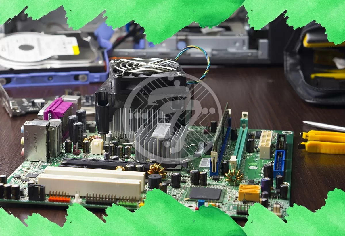
The use of Printed Circuit Boards has been ubiquitous across industries. Like with other industries, PCBs are also finding extensive application in the medical industry as more and more medical research and treatment methods become technology driven. With lives of patients at stake, it goes without saying that these devices are mission critical and that stringent guidelines need to be followed when it comes to Medical PCB Prototype. Clearly there cannot be an instance where there is a malfunctioning instrument when a critical, lifesaving medical procedure is being carried out. Little surprise then that these instruments need to be manufactured to some very exacting standards.
There need to be strong protocols related to PCB design, fabrication, PCB assembly, testing and inspection. Even though medical devices are varied, and their use is widespread across functions and there need to be specific standards and regulations related to their use, here is a quick overview of the broad Medical PCB Assembly Standards and Regulations:
IPC Standards
Presently called Association Connecting Electronics, its acronym comes from its former name i.e. Institute for Printed Circuits. It is an industry body that has issued a series of standards for circuit boards. These include:


- Harnesses
- Soldering
- Enclosures
- Cables


- The certification requires that all manufacturing phases are clearly documented so that products are built as per regulation
- It also ensures that processes are in place for risk management and design control.
- Manufacturers are also required to develop an audit system to track their own performance as far as the process goes.
With these standards in place, it is an assurance to regulators as well as to clients that the manufacturer is fully committed to quality and that it has the necessary systems as well as processes in place.
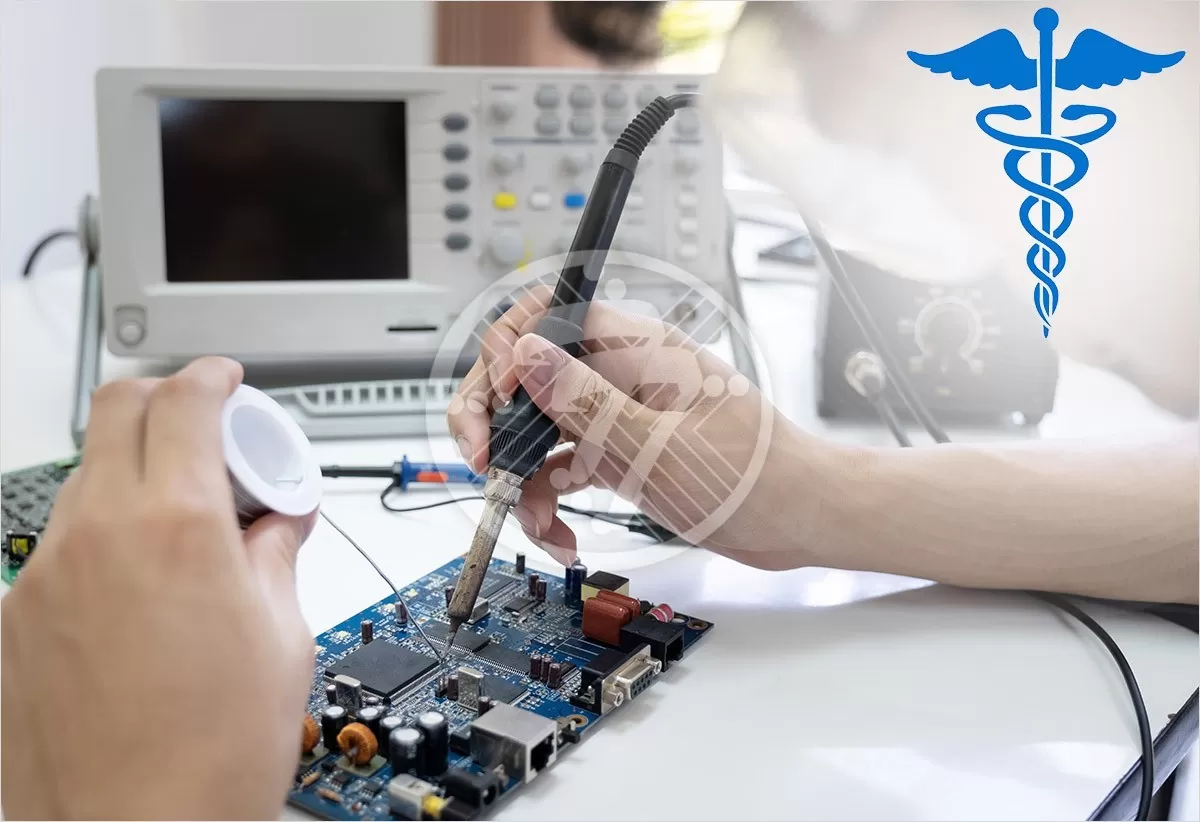
This of course, means that in order that your medical requirement meets the necessary regulatory standards, you need to partner with a contract manufacturer who works with these standards. If you have been looking for a contract manufacturer that offers Medical PCB Prototype that adheres to the highest standards, your search ends at Technotronix. Not only are we certified to the highest industry standards, but we also have a highly trained team that has the requisite experience and expertise when it comes to Medical Printed Circuit Board Assembly. The fact that we are also equipped with industry best practices ensures you do not need to reinvent the wheel. When you partner with us, you can rest assured that you will get medical equipment that stands tall against the exacting requirements.
TechnoTronix excels in providing solutions to medical mechanism. We offer medical electronic solutions to injection Molding and packaging and complete product manufacturing per layout. With over 4 decades of industry experience and rich knowledge to boot, little surprise then that Technotronix has emerged as a preferred partner of choice across industries including the Medical Printed Circuit Board Assembly.