Why and when you need to outsource electromechanical assemblies?


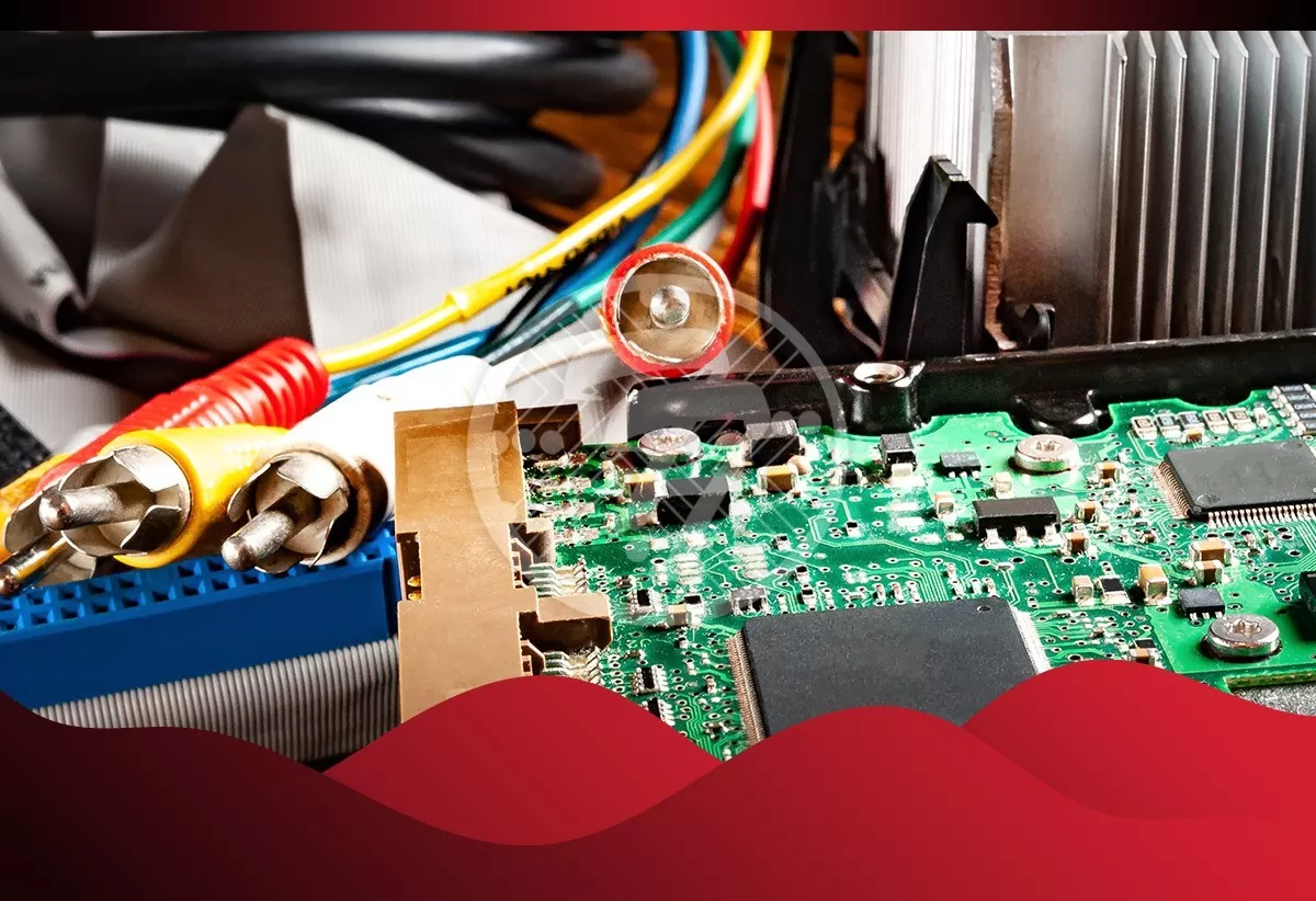
Electromechanical assemblies are increasingly becoming an integral part of major electronic products today. These are fairly complex assemblies comprising of circuit cards, custom cables and other electro-mechanical elements. For a product manufacturer, therefore, both capabilities as well as resources could undergo a severe strain in producing them. Manufacturers are therefore typically faced with a “build or buy” choice. The choices before you are clearly to either expend resources and competency mastering electromechanical assemblies or outsource it to people who have the necessary know-how and access to industry best practices to offer cutting-edge products.
One look at the numbers and it is clear that the scales tip in favor of outsourcing. The global market for electronic contract manufacturing is estimated to reach US$ 653.8 Billion by 2027 as per estimates by Strategy. Not without reason. There are many advantages of contract manufacturing PCB assembly. But here we are discussing outsourcing electromechanical assemblies, so its advantages are as follows:
Specialized Equipment
The first major advantage that contract manufacturers have is that of having state-of-the-art equipment. Whether it is wire cutting and crimping machine or a CNC mill, they invest in specialized equipment to build the assemblies. What they also have is rigorous testing protocols that ensure percentage of error is miniscule. For an OEM to invest in this kind of machinery and floor space for producing one component may not work out to be cost-effective at all.
It works far better for them to focus on their core competencies, and put that floor space to better use in creating the product that they produce, to increase their profitability.
Specialized Manpower
Once again, this is an area where contract manufacturers have an advantage. They recruit and train skilled manpower that specializes in Electronics Manufacturing Assembly Services. This kind of investment in manpower may not be worthwhile for an OEM.
Quality Processes
It is very important to having the quality checks in place when it comes to electro-mechanical assembly. This enables contract manufacturers to create assembly after assembly with the same level of precision. This ensures the OEM will receive products that are fully tested and it will ensure the efficacy of their final product. Typically, the kind of industry-best practices that a contract manufacturer has access to, is quite hard to replicate. With their existing relationships with suppliers, they also have the advantage of sourcing quality parts at the most cost-effective rates.
Additionally, with process certifications and training standards you can rest assured that what you will get is a high degree of reliability.
OEMs agree that it isn’t all that prudent to invest in people, expertise and equipment when you can get a good price as well as great turnaround times from a contract manufacturer. What it also saves them from is shouldering the additional in-house work.
The other reason why doing it in-house does not make sense is that contract manufacturers find it hard to scale up quickly. So, if the demand is for higher production volumes, it may be worth it, but, on the other hand, if the volume requirement is low, the investment in technology and manpower can be extremely hard to justify. A contract manufacturer however is fully equipped to handle full production runs as well as small quantities so contacting a contract manufacturer is a smart choice in both the cases.
Clearly then, outsourcing helps save both money and time that can be put to better use and expand your business portfolio further.
To sum up, what you get by outsourcing electro-mechanical assemblies are:
- A reliable product
- Cost-effective prices
- Quick turnaround time
All of this goes into the efficacy of your final product and gives you a tangible advantage of quick time-to–market. In a hugely competitive marketplace, the time spent in acquiring talent and infrastructure can put you considerably behind. With the contract manufacturer having the pre-existing competency for your requirements, quick time-to-market can be possible.
With the negative connotations around the term “outsourcing” no longer there, OEMs see it is as a necessary option. All you need to do is to choose your electronics contract manufacturer with care. You need to partner with the one who is committed to quality standards as well as quick turnaround times. Having identified such a contract manufacturer, what you have is not just a vendor of a sub assembly but your success partner.
Technotronix offers Electromechanical assembly services with 40 years of expertise. we take an extra step to reach out to your exact PCB requirements, high quality standards and strong customer support service to provide quick turnarounds and on-time delivery to our customers. In case if you have any questions, please feel free to contact us via email at sales@technotronix.us!