HASL vs ENIG vs OSP – What is the difference between optimal PCB surface finishes?
By | Date posted: | Last updated: July 29, 2025
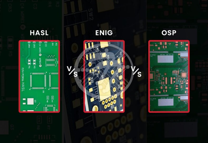
HASL vs ENIG Vs OSP

Choosing the right surface finish for a printed circuit board (PCB) is a vital step in achieving product reliability, solderability, and performance. Surface finishes such as HASL, ENIG, and OSP are not just protective layers – they influence electrical performance, assembly quality, environmental compliance, and even shelf life. Each finish serves a distinct purpose, making the decision especially important for industries like automotive, consumer electronics, aerospace, and medical devices.

In this blog, we break down the core differences between HASL, ENIG, and OSP surface finishes. We explore how they work, where they are best used, and what makes one better suited over the other depending on design goals and manufacturing demands.

What is HASL (Hot Air Solder Leveling)?

HASL, or Hot Air Solder Leveling, is one of the most used surface finishes in PCB manufacturing. It involves immersing the board in molten solder and then using hot air knives to remove excess solder from the surface. This creates a protective and solderable layer.

Advantages:

  • Economical and widely available across board houses.
  • Excellent solderability and ease of rework.
  • Reasonable shelf life when stored in controlled conditions.

Disadvantages:

  • Not suitable for high-density designs due to its uneven surface.
  • Thermal shock during the dipping process can damage sensitive boards.
  • The traditional version contains lead, making it non-compliant with RoHS standards unless a lead-free variant is used.

Typical Uses: Industrial boards, general-purpose electronics, and cost-sensitive designs that do not require very fine components.

What is ENIG (Electroless Nickel Immersion Gold)?

ENIG stands for Electroless Nickel Immersion Gold. It consists of a two-layer metallic coating where a layer of nickel is deposited chemically, followed by a thin coating of gold. The nickel acts as a barrier between the copper and gold, and the gold protects the nickel from oxidation.

Advantages:

  • Provides a very flat surface, ideal for fine-pitch components like BGAs.
  • Offers excellent corrosion resistance and long shelf life.
  • Compliant with RoHS regulations.
  • Suitable for applications requiring wire bonding.

Disadvantages:

  • Higher cost compared to other finishes.
  • Can be prone to a defect called black pad if not manufactured properly.
  • Requires tight process control and is harder to rework than HASL.

Typical Uses: High-density PCBs, telecom, aerospace, medical devices, and applications where reliability is paramount.

What is OSP (Organic Solderability Preservative)?

OSP, or Organic Solderability Preservative, is a water-based organic compound that is applied to exposed copper pads to prevent oxidation. It is one of the most environmentally friendly and low-cost surface finish options.

Advantages:

  • Very affordable and simple to apply.
  • Delivers a flat surface that supports fine-pitch soldering.
  • Environmentally friendly and RoHS compliant.

Disadvantages:

  • Shorter shelf life compared to other finishes.
  • Sensitive to handling and not suited for multiple reflow cycles.
  • Provides limited protection against corrosion or mechanical wear.

Typical Uses: Consumer electronics, single-reflow assembly processes, or PCBs with a short storage timeline.

Comparision Table of HASL vs ENIG vs OSP

Feature HASL ENIG OSP
Cost Low High Very low
Surface Flatness Uneven Very flat Flat
Fine-Pitch Support Poor Excellent Good
RoHS Compliance Lead-free only Yes Yes
Shelf Life 6–12 months 12–18 months 3–6 months
Rework ability High Moderate Low
Corrosion Resistance Moderate Excellent Low
Ideal Application Industrial/Low-end High-end/HDI Single-use consumer

Factors to consider when choosing a PCB surface finish

1. Design Complexity

For dense boards with small pitch components, ENIG offers the flattest and most reliable surface. HASL may introduce uneven surfaces that hinder solder joint integrity in such layouts.

2. Environmental Compliance

OSP and ENIG are both lead-free and compliant with environmental regulations. If you’re using HASL, ensure it’s the lead-free variant if compliance is required.

3. Cost Sensitivity

OSP is the most economical choice, followed by HASL. ENIG is the most expensive, but its reliability justifies the cost in complex applications.

4. Manufacturing Process Requirements

OSP is best for boards that undergo a single reflow process. For boards requiring multiple soldering cycles or long shelf life, ENIG is a better choice.

5. Mechanical Durability

ENIG is more robust and resistant to wear, making it suitable for boards that will be handled frequently or installed in rugged environments. OSP, by contrast, is delicate and should be handled carefully during assembly.

6. Storage Duration

If your product is expected to be stored for a long time before assembly, ENIG’s long shelf life makes it more reliable. OSP degrades quickly and is best suited for short manufacturing cycles.

Alternative Surface Finishes

While HASL, ENIG, and OSP are the most widely used, there are several alternative finishes:

  • Immersion Silver: Offers good solderability and flatness but tarnishes easily in high humidity.
  • Immersion Tin: Similar to silver but can suffer from tin whiskers over time.
  • ENEPIG (Electroless Nickel Electroless Palladium Immersion Gold): More reliable than ENIG, especially for wire bonding, but significantly more expensive.
  • Hard Gold: Used in edge connectors and high-wear contact areas, not typically used for soldering.

Each of these alternatives has a specific niche but is less commonly used for general-purpose boards.

Trends and Future Outlook

As electronics become smaller and more complex, the demand for flat, reliable surface finishes continues to rise. ENIG and OSP are seeing increased adoption in high-speed and high-frequency applications. Additionally, environmental regulations are shaping surface finish selection, driving a shift away from traditional leaded HASL.

Research and development are also underway to enhance existing finishes and create hybrid solutions that combine the benefits of multiple finishes. Advances in ENEPIG, for instance, aim to offer the performance of ENIG with fewer manufacturing risks.

Conclusion

Surface finish selection is a critical decision in PCB manufacturing. Whether you choose HASL, ENIG, or OSP depends on your specific application, budget, component density, and regulatory requirements. While HASL offers affordability and ease of use, it lacks the flatness and reliability needed for more complex assemblies. ENIG delivers superior performance but comes at a higher cost. OSP is an economical and eco-friendly choice, though it requires careful handling and fast processing.

By aligning surface finish choice with the board’s purpose and assembly process, you can optimize both manufacturing efficiency and long-term performance. Always consult your PCB fabricator for recommendations tailored to your project’s unique requirements.

Looking for the right PCB surface finish for your next project? At TechnoTronix, we combine decades of PCB manufacturing and fabrication expertise with advanced capabilities to deliver the finish that best fits your application – whether it’s HASL, ENIG, or OSP. Get in touch with our team at [email protected] to discuss specific needs and receive a reliable, high-performance solution.

What is the role of UPS PCBs in data centers, hospitals, and industrial automation?

By | Date posted: | Last updated: July 1, 2025
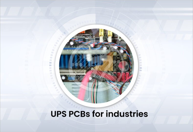
UPS PCBs for industries

In a world that thrives on uninterrupted connectivity, consistent power is more than convenience—it’s a lifeline. From the relentless demands of data centers to the life-critical operations of hospitals and the precision-driven realm of industrial automation, power reliability is non-negotiable. At the center of this reliability is the Uninterruptible Power Supply (UPS)—and more specifically, the Printed Circuit Boards (PCBs) within these systems that quietly manage, control, and safeguard the flow of electricity.

UPS PCBs might not get the spotlight, but they are the brains behind every successful power backup operation. Whether its keeping servers running during a blackout, powering surgical equipment during an outage, or ensuring production lines never falter, UPS PCBs are the unsung heroes of modern infrastructure. This blog explores their roles in detail and shows why they matter so much in high-stakes environments.

1. Understanding UPS and their PCBs

A UPS provides backup power during interruptions—ranging from milliseconds-long brownouts to full blackouts. Most modern UPS systems—especially those used in critical industrial applications—are online for double-conversion designs. In these, incoming AC power is rectified to DC, charges the battery, and then inverted back to clean AC for the load.

At the core of these functions are specialized PCBs, responsible for:

  • Rectifier boards that control AC-to-DC conversion.
  • Inverter boards that transform battery power back into AC.
  • Control logic boards that manage transitions, monitor load, and communicate status.
  • Power conditioning modules provide voltage regulation and surge protection.

High-quality PCBs ensure stable power transformation, efficient operation, and systems that meet uptime requirements—even during complex failure scenarios.

2. Role in Data Centers

a. Ensuring Zero-Downtime Operations

Data centers demand constant power – any interruption risks lost data, hardware damage, or downtime costing thousands per minute. UPS PCBs enable:

  • Continuous power quality management, smoothing voltage fluctuations, and preventing transient damage.
  • Instantaneous transfer to battery power during outages, facilitated by controlling PCBs coordinating rectifiers, inverters, and static bypass switches.
  • Support for scalable, modular systems (e.g. N+1 redundancy). PCBs enable hot-swappable and parallel configurations to maintain uptime during expansion or maintenance.

b. Advanced Grid Services

Beyond backup, UPS systems can actively support the power grid using advanced features programmed into their PCBs:

  • Demand response—shifting load from grid to batteries during peak demand.
  • Grid frequency regulation—absorbing or injecting power to stabilize 60 Hz fluctuations.
  • Energy arbitrage—storing electricity when cheap and feeding it back when rates are high.

These functions rely on embedded firmware and sophisticated control algorithms on PCBs—transforming UPS units from passive backups into active grid assets.

3. Hospitals: Power Protection with Patient Safety in Mind

In healthcare settings, power reliability correlates directly to patient lives—making UPS systems critical, and their PCBs even more so.

a. Safe Handover to Life-Saving Systems

Hospital UPS units maintain power to:

  • Life-support machines, imaging systems, and ventilators.
  • Critical monitoring and safety equipment during generator transitions

Control PCBs ensure zero-break transitions, prevent electrosurgical noise, and maintain clean voltage for sensitive medical instruments.

b. Rigorous Safety and Compliance

Hospital-grade UPS PCBs include:

  • Redundant protection circuits to prevent single-point failures.
  • Isolation and EMC filters to reduce electrical interference with medical devices.
  • Monitoring and alarms tied into building systems to swiftly report faults.

PCB-level reliability and regulatory certification underlie hospital safety systems—critical in emergencies.

4. Industrial Automation: Reliable Power for Production

In industrial environments, automation lines and control systems cannot tolerate power fluctuation or failure.

a. Protecting Control Systems

UPS systems keep PLCs, HMIs, and automated lines powered during brownouts or outages. PCB functions include:

  • Power smoothing and voltage control to prevent malfunctions or resets.
  • Fast transfer to stored power to maintain production flow.
  • Pre-shutdown routines allowing controlled halting of motors and robots.

b. Onsite Conditioning and Control

Industrial-grade UPS PCBs often integrate:

  • EMI/RFI filtering to handle noisy industrial power lines.
  • Programmable signal interfaces for SCADA/BMS integration.
  • Robust certifications to endure heat, dust, and vibration common in manufacturing spaces.

c. Maintenance and Decommission Management

These PCBs provide:

  • Diagnostic modules that identify battery degradation or board faults.
  • Modular designs enabling field replacement and minimal downtime.

5. Shared Benefits Across Applications

While the environments differ, UPS PCBs provide critical capabilities across all sectors:

  • Power Conditioning: Rectifier/inverter boards clean and maintain voltage quality.
  • Seamless Switching: Static bypass and smart control logic eliminate delays.
  • Battery Management: PCBs manage charging, discharge control, and health monitoring.
  • Redundancy & Scalability: Modular PCBs support hot-swappable units and parallel operations.
  • Diagnostics & Maintenance: Embedded sensors and alert systems preempt failures.
  • Grid Integration: Firmware enables UPS systems to act as grid assets.
  • Safety & Compliance: Isolation, filtering, and fail-safes ensure regulatory standards are met.

6. The Future: Smarter, Leaner, More Capable PCBs

As technology evolves, key trends in UPS PCB design include:

  • Lithium-ion battery support, offering faster recharge cycles and higher energy density
  • IoT-enabled monitoring, with remote alerts, analytics, and firmware updates.
  • More compact designs using high-power-density components and optimized thermal layouts.
  • Sustainable energy use, enabling microgrid and renewable integration via PCB control systems.

These advances promise UPS units that are smarter, greener, and more responsive.

Conclusion

In mission-critical environments, there is no room for error when it comes to power supply. UPS PCBs are not just components—they are the backbone of intelligent, resilient, and responsive backup power systems. Their design and functionality are the reasons hospitals continue surgery during blackouts; data centers avoid catastrophic downtime, and industrial lines maintain continuous production even when the grid falters.

As industries evolve and demand smarter, more efficient energy solutions, the role of UPS PCBs will only grow more vital. They’re becoming more compact, intelligent, and capable of integrating with modern digital ecosystems. Whether you’re responsible for IT uptime, patient safety, or manufacturing efficiency, understanding the importance of UPS PCBs means being a step ahead in securing uninterrupted performance.

Reliable power begins with smart design—and that design starts with a UPS PCB.

Looking to enhance the reliability and performance of your UPS systems? We deliver high-quality, custom UPS printed circuit board manufacturing to meet the critical demands of data centers, hospitals, and industrial automation environments. Reach out [email protected] today to discuss your project needs and discover how our advanced PCB solutions can support uninterrupted power and operational efficiency where it matters most.

RoHS Compliance in PCB Manufacturing: Top essential questions for your EMS provider!

By | Date posted: | Last updated: January 16, 2025
RoHS compliance in PCB manufacturing

As environmental regulations tighten globally, compliance with the Restriction of Hazardous Substances (RoHS) directive has become a cornerstone of sustainable electronics manufacturing. RoHS aims to limit the use of hazardous materials in electronic and electrical equipment, ensuring environmental safety and user health. If you are working with an Electronics Manufacturing Services (EMS) provider for PCB production, it is crucial to evaluate their RoHS compliance strategy.

Here are five critical questions to ask your EMS provider to ensure smooth, compliant, and efficient production.

1. What measures do you take to ensure RoHS Compliance?

Understanding your EMS provider’s compliance strategy is vital. Ask about their processes for sourcing RoHS-compliant components, managing supply chains, and adhering to updated regulations like RoHS 2 and RoHS 3. The latest standards, such as Directive 2015/863 (RoHS 3), restrict ten hazardous substances, including lead, mercury, cadmium, and four phthalates.

Ensure your provider employs robust tracking and reporting systems for materials and maintains detailed documentation for auditing purposes. Key tools, such as XRF analyzers for material testing, are essential for verifying compliance.

2. Are your suppliers verified for RoHS-Compliant Components?

The reliability of your EMS provider’s supply chain significantly impacts compliance. Non-compliant suppliers could result in recalls, fines, or brand damage. A reliable EMS provider collaborates only with certified suppliers who follow RoHS guidelines and conducts periodic audits to verify materials’ safety.

Request details about supplier selection criteria and how they avoid hazardous substances in raw materials. Proper sourcing practices prevent contamination and ensure full compliance.

3. How do you handle exemptions and updates to RoHS Directives?

Certain applications may qualify for exemptions under RoHS, such as medical devices or military electronics. However, managing exemptions requires expertise to ensure that they are valid, and that compliance is maintained elsewhere.

Additionally, the RoHS landscape evolves, with updates like RoHS 4 potentially on the horizon. A forward-thinking EMS provider will keep pace with these changes, proactively adapting processes and helping you plan for future compliance requirements.

4. What testing protocols do you follow for PCB products?

Testing is non-negotiable in RoHS-compliant PCB manufacturing. Ask about the specific methods your EMS provider uses to verify compliance. Portable X-ray fluorescence (XRF) analyzers are widely used to detect restricted metals in PCB components.

Moreover, inquire whether they perform batch testing or continuous monitoring and how often equipment is calibrated to ensure accuracy. Reliable testing prevents non-compliance issues that could arise post-manufacturing.

5. Do You Provide Full Documentation for RoHS Compliance?

Proper documentation is integral to RoHS compliance. Your EMS provider should furnish production records, including material sourcing, testing data, and compliance certifications. These records are crucial for audits, especially in regions requiring CE marking and detailed conformity assessments, like the European Union.

Ensure your provider retains records for the mandated 10-year period and offers easy access to documentation if needed for regulatory inspections.

Why RoHS compliance matters for PCB manufacturing?

Failing to meet RoHS standards can have severe consequences, including legal penalties, product recalls, and damage to your company’s reputation. More importantly, adherence to these standards reflects a commitment to environmental responsibility and customer safety. With the EU and other regions prioritizing stringent compliance checks, RoHS adherence is not just a regulatory box to tick – it is a competitive advantage.

Conclusion

When selecting an EMS provider for RoHS-compliant PCB manufacturing, don’t just focus on cost or production speed. Their commitment to regulatory compliance, ability to adapt to changes, and transparent practices are equally critical. Asking these five essential questions will help you identify a partner who ensures PCBs meet the highest standards of quality and environmental safety.

By integrating RoHS compliance into your manufacturing strategy, you can minimize risks, foster innovation, and ensure sustainable growth in the electronics industry.

Looking for reliable RoHS-compliant PCB manufacturing? At Technotronix, we specialize in delivering eco-friendly, high-quality PCBs tailored to meet your needs. Partner with us for unparalleled expertise, advanced technology, and a commitment to sustainability.

Contact us today at [email protected] to discuss your project and ensure compliance every step of the way!

Designing and Manufacturing PCBs for Enterprise IoT Applications: Key Considerations and Best Practices

By | Date posted: | Last updated: December 24, 2024
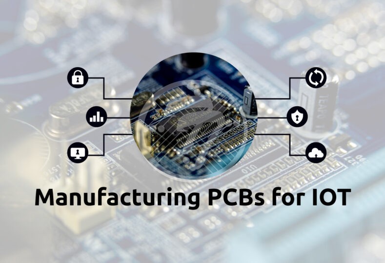
Manufacturing PCBs for IOT

As the Internet of Things (IoT) continues to revolutionize industries, enterprise applications increasingly rely on custom-designed printed circuit boards (PCBs) for their hardware needs. These PCBs act as the backbone of IoT devices, facilitating connectivity, processing, and data transfer. Designing and manufacturing PCBs for enterprise IoT applications, however, demands careful planning and execution to ensure reliability, scalability, and cost-effectiveness.

This article delves into the key considerations and best practices for creating PCBs tailored to enterprise IoT environments, offering insights into the unique challenges posed by IoT devices and the strategies to overcome them.

Key Considerations in Designing PCBs for IoT Applications

1. Application-Specific Design Requirements

Enterprise IoT applications span diverse industries such as healthcare, manufacturing, agriculture, and logistics. Each use case brings specific requirements regarding size, weight, durability, and functionality. For example:

  • Healthcare IoT devices need miniaturized PCBs with high reliability to fit within wearable medical devices.
  • Industrial IoT (IIoT) sensors may require rugged PCBs capable of withstanding harsh environments, including high temperatures and vibrations. Understanding these requirements from the outset helps align design choices with end-use needs.

2. Power Efficiency

IoT devices often operate on limited power sources, such as batteries or energy harvesting systems. The PCB design must prioritize:

  • Low power consumption: Use low-power components and efficient power distribution paths.
  • Power management ICs: Implement regulators and capacitors to stabilize power flow. Power efficiency is critical in ensuring the longevity of IoT devices, particularly for remote or hard-to-access installations.

3. Connectivity and Signal Integrity

Enterprise IoT applications rely on wireless connectivity protocols like Wi-Fi, Bluetooth, Zigbee, and LoRa. The PCB must support robust communication, which involves:

  • Minimizing interference through effective layout design.
  • Ensuring proper antenna placement to avoid signal attenuation.
  • Managing signal integrity by reducing crosstalk and electromagnetic interference (EMI) through trace routing techniques.

4. Environmental Factors

IoT devices in enterprise environments face exposure to challenging conditions, such as dust, moisture, or extreme temperatures. PCBs must incorporate:

  • Conformal coatings to protect against moisture and corrosion.
  • Materials with appropriate thermal management properties to dissipate heat effectively.
  • Design practices that comply with standards such as IP ratings for water and dust resistance.

5. Scalability and Cost Considerations

Enterprise IoT applications often demand scalability. When designing PCBs, consider:

  • Panelization strategies maximize manufacturing efficiency.
  • Choosing cost-effective materials and components without compromising quality.
  • Ensuring the design can be easily adapted or upgraded for future iterations.

Best Practices for PCB Design in Enterprise IoT!

1. Collaborate Early with Stakeholders

Engage all stakeholders—including product managers, software engineers, and end-users—early in the design process. Collaboration ensures the PCB design meets functional and operational requirements while avoiding costly redesigns later.

2. Adopt Design-for-Manufacturing (DFM) Principles

Design for manufacturing principles optimize the design to minimize manufacturing complexities. Key practices include:

  • Avoiding tight tolerances where unnecessary.
  • Simplifying via placement to reduce drilling costs.
  • Standardizing component packages to streamline assembly.

3. Implement Advanced Simulation Tools

Use simulation tools to test PCB designs virtually before prototyping. Simulations help identify issues such as thermal hotspots, EMI, or signal loss, enabling designers to address them early.

4. Focus on Prototyping and Iteration

Prototyping allows you to test designs in real-world conditions. Perform multiple iterations to refine the PCB for performance, durability, and manufacturability. Rapid prototyping techniques, such as 3D printing, can expedite this process.

5. Optimize for Wireless Performance

For IoT applications, antenna design is critical. Ensure:

  • Proper impedance matching between the antenna and PCB traces.
  • Isolation of the RF section to reduce noise.
  • Use of simulation tools specific to RF design.

6. Prioritize Security Features

Enterprise IoT devices must safeguard sensitive data. PCB design should support:

  • Hardware encryption modules.
  • Secure boot mechanisms.
  • Tamper-detection circuits.

7. Emphasize Sustainability

Design eco-friendly PCBs by selecting recyclable materials and reducing waste during manufacturing. Compliance with standards like RoHS (Restriction of Hazardous Substances) and WEEE (Waste Electrical and Electronic Equipment) can enhance sustainability.

Key considerations in PCB manufacturing for IoT

1. Material Selection

Choose PCB materials based on the application’s performance requirements. For example:

  • FR-4 laminates are cost-effective for general-purpose IoT devices.
  • High-frequency materials like Rogers laminates are ideal for devices requiring superior signal performance.

2. Layer Stack-Up

IoT PCBs often require multiple layers to accommodate complex routing and shielding. Work with manufacturers to determine an optimal stack-up configuration balancing performance and cost.

3. Precision in Component Placement

Automated pick-and-place machines are used in PCB assembly to ensure accurate component placement. Design the PCB with clear fiducial marks and proper spacing for automated processes.

4. Testing and Quality Control

Enterprise IoT applications demand high reliability. Use testing methods like:

  • In-Circuit Testing (ICT): Verifies electrical connections.
  • Functional Testing (FT): Ensures the PCB performs as intended.
  • Environmental Stress Testing (EST): Simulates real-world conditions to test durability.

Find out the difference between In-Circuit Testing and Functional Testing.

5. Partnering with Reliable Manufacturers

Choose manufacturers with experience in IoT PCB production. Evaluate their capabilities in terms of:

  • Advanced equipment for fine-pitch and high-density designs.
  • Certifications such as ISO 9001 and IPC standards.
  • Track record of delivering high-quality, scalable solutions.

Case Study: PCB Design for Industrial IoT Sensors

A company developing IoT-enabled vibration sensors for industrial machinery required PCBs that were compact, durable, and power-efficient. Key steps included:

  • Choosing rigid-flex PCBs to fit within small housings.
  • Incorporating low-power microcontrollers to extend battery life.
  • Adding conformal coatings for protection against oil and dust.
  • Collaborating with the manufacturer to ensure scalability for mass production.

This approach resulted in a robust product capability of withstanding industrial environments while meeting customer requirements.

Future Trends in IoT PCB Design and Manufacturing

  1. Miniaturization: As IoT devices become smaller, advancements in PCB technology will focus on compact, high-density designs using techniques like HDI (High-Density Interconnect).
  2. Integration with AI and Machine Learning: Future PCBs may include on-board AI chips, enabling real-time data analysis for IoT applications.
  3. Advanced Materials: Graphene-based PCBs and flexible substrates could revolutionize durability and form factor.
  4. Sustainability Efforts: Emphasis on recyclable materials and energy-efficient manufacturing processes will continue to grow.

Conclusion

Designing and manufacturing PCBs for enterprise IoT applications involves a delicate balance of technical expertise, strategic planning, and collaboration. By addressing key considerations such as power efficiency, connectivity, and environmental resilience, and adhering to best practices like DFM and advanced simulation, developers can create reliable and scalable solutions.

As IoT continues to reshape industries, staying ahead in PCB technology will be pivotal in unlocking the full potential of enterprise IoT applications.

Looking to bring your IoT innovations to life with reliable PCBs? At TechnoTronix, we specialize in designing and manufacturing high-performance PCBs tailored for enterprise IoT applications. With advanced capabilities and a focus on quality, we deliver solutions that enhance connectivity, durability, and efficiency. Partner with us to meet your IoT PCB needs and ensure your devices excel in performance. Get in touch with us at [email protected] to explore custom PCB solutions!