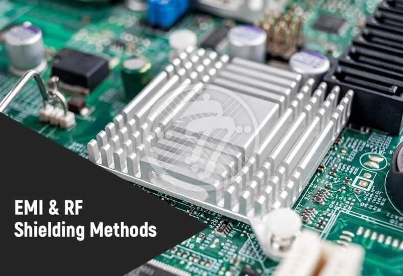
Top EMI and RF Shielding Methods for Custom Flexible PCB!

Custom Flex PCBs are subject to both Electromagnetic as well as Radio Frequency Interference. In turn, this can lead to a whole lot of consequences including but not limited to an increase in error rates.
To protect custom flexible PCBs against this interference, it is important to carry out EMI shielding. This can be done by way of copper layers, silver ink and shielding films, each of which comes with a distinct set of advantages and disadvantages.
Let us look at the process in some detail as also look at the selection parameters:
What is EMI and RF shielding?
It is a method that prevents electromagnetic and radio frequency interference from external signals.
In addition, it prevents high-frequency signals from leaking out. This is done by using metallic barriers. Essentially the shielding effect is based on a principle used in Faraday Cage, which is that the metallic screen surrounds the sensitive or transmitting electronics.
In selecting the type of EMI shielding, it important to consider the following two aspects, namely the bend requirements and the controlled impedance.
Bend requirements
The minimum bend capacity is a function of the thickness. It can, therefore, reduce the bending capacity of the PCB. It is important, therefore, to evaluate the minimum bend radius and bend type requirements for shielded designs. Another aspect to consider includes whether the bend required is static or dynamic. It is important to remember that the bending capacity of a dynamic flex circuit board is far higher than that of a static one.
Controlled impedance
In Flexible PCB Board, the controlled impedance signal requirements also impact the EMI & RF shielding approach. The shields need to have electrical properties that meet the necessary criteria to obtain the appropriate impedance values.
Types of EMI & RF shielding used in Custom Flexible PCB
EMI shielding is done using 3 types of materials, namely:
- Copper Layers
- Silver Ink
- Shielding Films
In making the choice of material, some of the considerations include:
- Shielding Performance
- Mechanical Bend Capabilities
- Suitability for controlled impedance
Copper Layers
Here the copper layers are used either as solid or cross-hatched planes. They are linked to the ground through stretched vias. The solid copper layers tend to provide a higher degree of shielding. Cross-hatched layers, on the other hand, are used where shielding is required without impacting the board flexibility.
The disadvantage of this shielding, stems from the fact that it increases the thickness which in turn affects the bending capacity. In fact a three-layer copper shielded flex circuit increases the thickness by nearly 125%.
Also, the fact that the shielding layers are connected to the ground plane through vias, tends to act as a mechanical stress concentrator.
Silver ink
As opposed to copper layers, silver ink has the advantage of offering greater flexibility at a lower cost. A silver ink shielded flex circuit is only about 75% thicker. Additionally, silver ink uses selected perforations in the coverlay. These perforations, in turn, allow for electrical interconnections.
Also, silver ink is relatively inexpensive as compared to other shielding material.
Specialized shielding films
These are suitable for dynamic bend applications and are suited for small structures. These also work well in sensitive applications.
Essentially it involves an electrically conductive adhesive, a metallic layer, and an insulating layer to be laminated. It is then bonded on the surface of the coverlay.
In terms of thickness, a 2-sided shielded film is only 15-20% thicker.
What are some of the design tips to avoid EM and RF interference in Custom Flexible PCB Boards?
- Sharp bends need to be avoided as they lead to fluctuations in impedance and signal reflections.
- It is important to isolate high-speed and low-speed signals.
- It is imperative that the current return path be kept small
- Vias should not be placed in differential pairs
- If split ground planes are required, they should be connected at a single point
To sum up
To ensure that the shielding is reliable and cost-effective, it is important to undertake a thorough examination of all aspects of the electrical and mechanical design factors. This will help in arriving at the right shielding method that works well for your Flex PCB.
At Technotronix, we are fully equipped to handle your PCB manufacturing requirements. With state-of-the-art equipment, we deliver the highest quality boards that you can rely on. No matter how complex your requirement, you can count on us to deliver to your bespoke needs. Our stringent quality control processes ensure that the boards deliver to your benchmarks.
To get more insights into the PCB fabrication, multilayer PCB fabrication & quick turn PCB fabrication, please explore our PCB fabrication services. Also, you can drop an email to [email protected] to solve your queries or to get a quote for custom flexible circuit boards, rigid-flex PCBs, flexible printed circuit boards manufacturing, flexible PCB prototyping.


