How to get an accurate quote for turnkey electronics manufacturing?


In today’s fast-paced world of electronics manufacturing, securing an accurate quote is the crucial first step towards turning your innovative ideas into reality. Turnkey electronics manufacturing and assembly offers a comprehensive solution that streamlines the entire process, from design to production and assembly, all within a single, efficient framework. This article is your guide to understanding the ins and outs of obtaining precise quotes for your turnkey electronics manufacturing needs.
What’s included in turnkey PCB manufacturing?
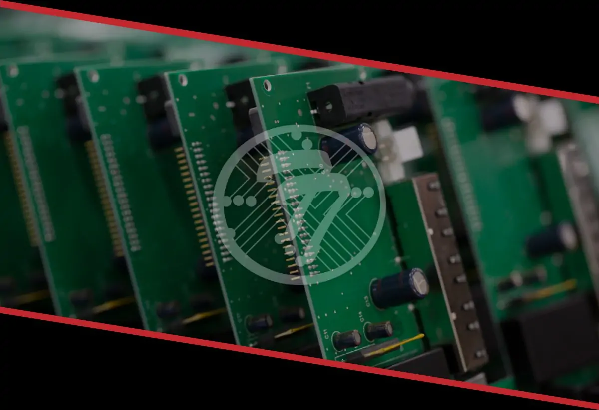
Turnkey PCB manufacturing and assembly refers to a comprehensive solution that streamlines the entire process of creating printed circuit boards (PCBs) for electronic devices, from design to fabrication and assembly, all under one roof. This approach is particularly beneficial for innovative small businesses, startups, and medium-sized companies, as it helps them overcome various challenges, they might face in the PCB assembly process. Key components of turnkey PCB manufacturing and assembly include:
- Design Support: Turnkey service providers often help with PCB design, ensuring that the circuit board is optimized for the intended application. This can involve optimizing component placement, trace routing, and other design considerations.
- PCB Fabrication: This involves the production of the PCB substrate, copper layer etching, drilling of holes, and other processes necessary to create the physical circuit board.
- Component Sourcing: Turnkey services typically handle the procurement of electronic components required for the PCB assembly. They maintain relationships with suppliers and ensure the availability of components needed for the project.
- PCB Assembly: This is a crucial step where electronic components are soldered onto the PCB. Turnkey providers have the expertise and equipment to handle surface-mount and through-hole components, as well as complex assembly processes.
- Testing and Quality Control: Turnkey solutions often include rigorous testing procedures to ensure the assembled PCBs meet quality and performance standards. This helps prevent defects and ensures that the final product functions correctly.
- Logistics and Shipping: Once the PCBs are assembled and tested, turnkey service providers can manage the logistics of shipping the finished products to the customer, which can be particularly convenient for businesses.
What are the benefits of turnkey PCB manufacturing?
- Time Efficiency: Turnkey services offer shorter lead times by consolidating all the steps in the PCB production process. This allows businesses to bring their products to market faster.
- Cost-Effective: By leveraging the service provider’s expertise and economies of scale, businesses can often reduce costs associated with inventory management, equipment investment, and labor.
- Quality Assurance: With comprehensive quality control measures, turnkey solutions minimize the risk of defects and errors, resulting in a higher-quality product.
- Reduced Complexity: Small businesses and startups can focus on their core competencies while leaving the complexities of PCB manufacturing and assembly to experts.
- Scalability: Turnkey services can accommodate small to medium-volume production, making them suitable for businesses with varying production needs.
Follow the steps to get an accurate quote for turnkey electronics manufacturing:
- Bill of Materials (BOM) and Gerber Files:
- Prepare a comprehensive Bill of Materials that includes raw materials, components, and critical production information. Ensure it is in a Microsoft Excel spreadsheet format.
- Allow for alternates for common capacitors and resistors.
- Share Gerber files and PCB fabrication drawings, which should include essential details like board dimensions, thickness, layer count, and part numbers. Ensure Gerber files are in standard formats (RS-274X, RS-274-D, DXF, DWG).
- PCB Testing Requirements:
- Clearly indicate your preferred PCB testing options, such as conformal coating, lot tracking, RoHS compliance, etc.
- Inspection Requirements:
- Specify any inspection requirements for your assembly, including X-ray, automated optical inspection (AOI), and flying probe tests.
- Inform the electronics contract manufacturer (ECM) of the industry-specific or IPC-regulated standards your assemblies need to meet.
- Quantities and Release Sizes:
- Include details on order quantity, estimated annual usage, and the first delivery date.
- If you require quick-turn prototypes, clearly state this requirement.
- Additional Information:
- Reach out to your ECM for clarification if you are unsure about any information they require. Different ECMs may have specific requirements.
- Consider working with a local ECM in the USA to streamline communication and services.
- Type of Turnkey Service:
- Decide whether you need full turnkey service (where the ECM orders all parts) or partial turnkey service (where you arrange for some components). Provide the relevant information accordingly.
- Lead Time and Cost Considerations:
- Understand the lead time for your specific type of turnkey assembly (full or partial).
- Be aware that shorter turn times may come at a higher cost.
- Consider the shipping costs, especially for urgent deliveries.
- Request for Quote:
- Submit all the necessary information to the ECM.
- Many ECMs provide quotes within 1 to 2 days of receiving complete information.
- Consider Procurement Efficiency:
- Some ECMs may offer cost savings for larger volumes of orders.
- Evaluate whether ordering in larger volumes aligns with your project needs and budget.
By following these steps and providing detailed information in the format recommended by the ECM, you can increase the chances of receiving an accurate quote for turnkey electronics manufacturing. Clear communication and collaboration with the ECM are essential to ensure that the quote meets your project requirements and expectations.
Conclusion
Navigating the realm of turnkey electronics manufacturing requires a systematic approach, attention to detail, and clear communication with your chosen electronics contract manufacturer. As the demand for electronics continues to surge, harnessing the power of turnkey manufacturing is the key to bringing your electronic innovations to life with efficiency and precision.
TechnoTronix offers full, partial, consigned, and kitted turnkey electronics PCB assembly services at the best price and in the best possible time. Request a turnkey PCB assembly quote or reach out at email sales@technotronix.us or call 714/630-9200.