Top Benefits of Contract Manufacturing PCB Assembly in USA!


Having an experienced third party contract PCB Manufacturing service is a source of major competitive advantage. While electronics manufacturers may have the ability to design boards and the skills to assemble the final product, they typically do that have the experience to manufacture boards. For them to get into board manufacturing would mean trying to reinvent the wheel. A contract PCB manufacturing service, on the other hand has a huge body of industry knowledge that you can benefit from. Besides some of the other advantages you can reap involve reduced overhead costs as well as the ability to focus on your core competencies.
Before we get into the details of the numerous advantages offered by contract PCB manufacturing, it will be worthwhile to get into some details of what third party contract manufacturing actually entails.
What exactly is third party contract manufacturing PCB assembly?
A third party or contract manufacturer, across industries, is one that builds products under the other company’s brand name. When it comes to PCB manufacturing, a contract manufacturer builds custom boards basis the designs of the company that has contracted its services. With the skill and expertise of the PCB manufacturer, the electronics manufacturer tends to gain in terms of reliability as a PCB is imperative to the success of the final product.
Following are the advantages of Contract PCB Manufacturing service:
Makes the process easy
Building your own PCB comes with a wide range of difficulties including but not limited to:
- Expenses involved in purchasing and maintain state-of-the-art equipment.
- Having robust processes in place
- Having to employ experienced and skilled staff who is capable of handling complex PCB fabrication & assembly.
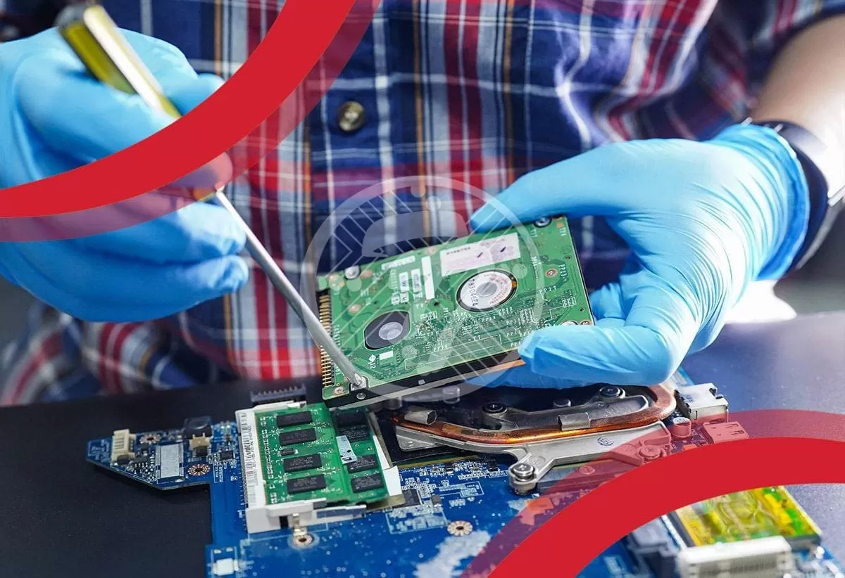
On the other hand, with a contract manufacturer you will be assured of the fact that he has both the equipment and expertise required to deliver quality products. Importantly they have a lot of experience in making sure that your design can be manufactured efficiently. Additionally the experienced staff is fully equipped to handle boards that are multi layered and have high density of components. In a scenario where miniaturization is a growing trend, the importance of this cannot be overstated.
Product quality
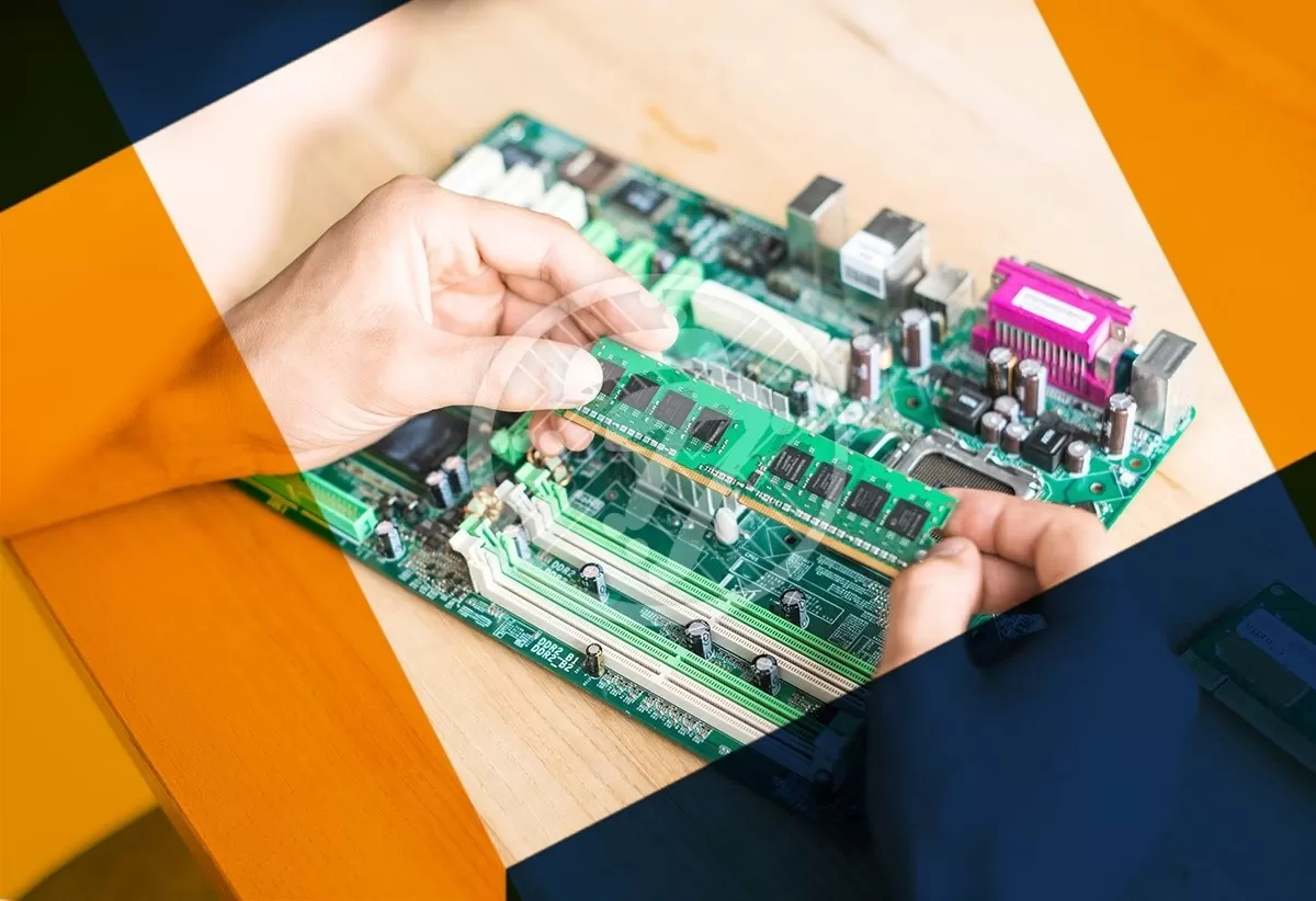
For an electronics manufacturer, the quality of the boards is paramount as it impacts the quality of their final products as also their company reputation. With a PCB contract manufacturer, experienced engineers focus on the manufacturability of each design. Also, PCB contract manufacturers have a host of industry certifications and quality standards to live up to. All of this ensures that the quality of boards that you get live up to the latest industry standards.
Optimal Costs
With a contract manufacturer another big advantage you have is that they have a wide network of vendors. What this means, is that they can secure quality components at the best price. For components that aren’t readily available they are also trained to make alternate recommendations that will not come in the way of the quality of the product.
Capability to produce low volume PCB prototype
Oftentimes, you would want low volume prototypes designed, to be able to gauge at the final product, without investing in a full production run, just yet. With the USA based PCB manufacturer, you have at your disposal the capability to get low volume production runs with the same unstinting focus on quality.
Quick turnaround time for PCB assembly
What a contract manufacturer also offers is quick turnaround time. With quick go-to-market being a significant source of competitive advantage, the importance of this cannot be overstated.
For an electronic manufacturer, therefore, trying to build the boards themselves can turn out to be a costly mistake. Not only will it add a whole lot of overheads to the operations, importantly even after that you cannot be sure of the quality of the boards. While you can replicate the machines, what will be hard to replicate is the body of experience that the contract manufacturer has. It is this experience that allows him to correct many mistakes early, which if detected after the production run can be really expensive. The expense isn’t in terms of money but can also be in terms of company reputation that is extremely hard earned.
Technotronix offer high quality and defect free PCB Assembly and PCB manufacturing services as per customer specification. We also offering dedicated SMT PCB Assembly, Prototype PCB Assembly, Led PCB Assembly, Overseas PCB Assembly, Mastering Mixed PCB Assembly and more services as per customer requirements and specification. In case if you have any questions, please feel free to contact us via email at sales@technotronix.us