Some of the biggest influences that affect PCB Manufacturing Cost


When it comes to Printed Circuit Board Assembly, there are a host of factors that determine its cost. Beginning with the technology used to the number of components, there are an array of aspects that directly impact the cost. However what is often forgotten are a number of indirect factors that also add to the PCB Assembly Cost. These factors include areas such as lack of testing equipment for example or even lack of trained manpower. Best practices such as lack of Design for Assembly as well as design for Manufacturing can also go a long way in positively impacting efficiency and negatively impacting cost. At the design stage itself, components need to be chosen with utmost care. Similarly the placement of these components can have a bearing on costs. Ensuring that you Design for Manufacturing, for example also goes a long way in eliminating issues at the design stage itself, as well as keeping costs under control. If not done correctly, aspects such as the design and placement of components could significantly affect costs. Check out the guide on how to reduce PCB assembly cost.
Here is a quick overview of some of the factors that impact PCB Manufacturing Cost:
-
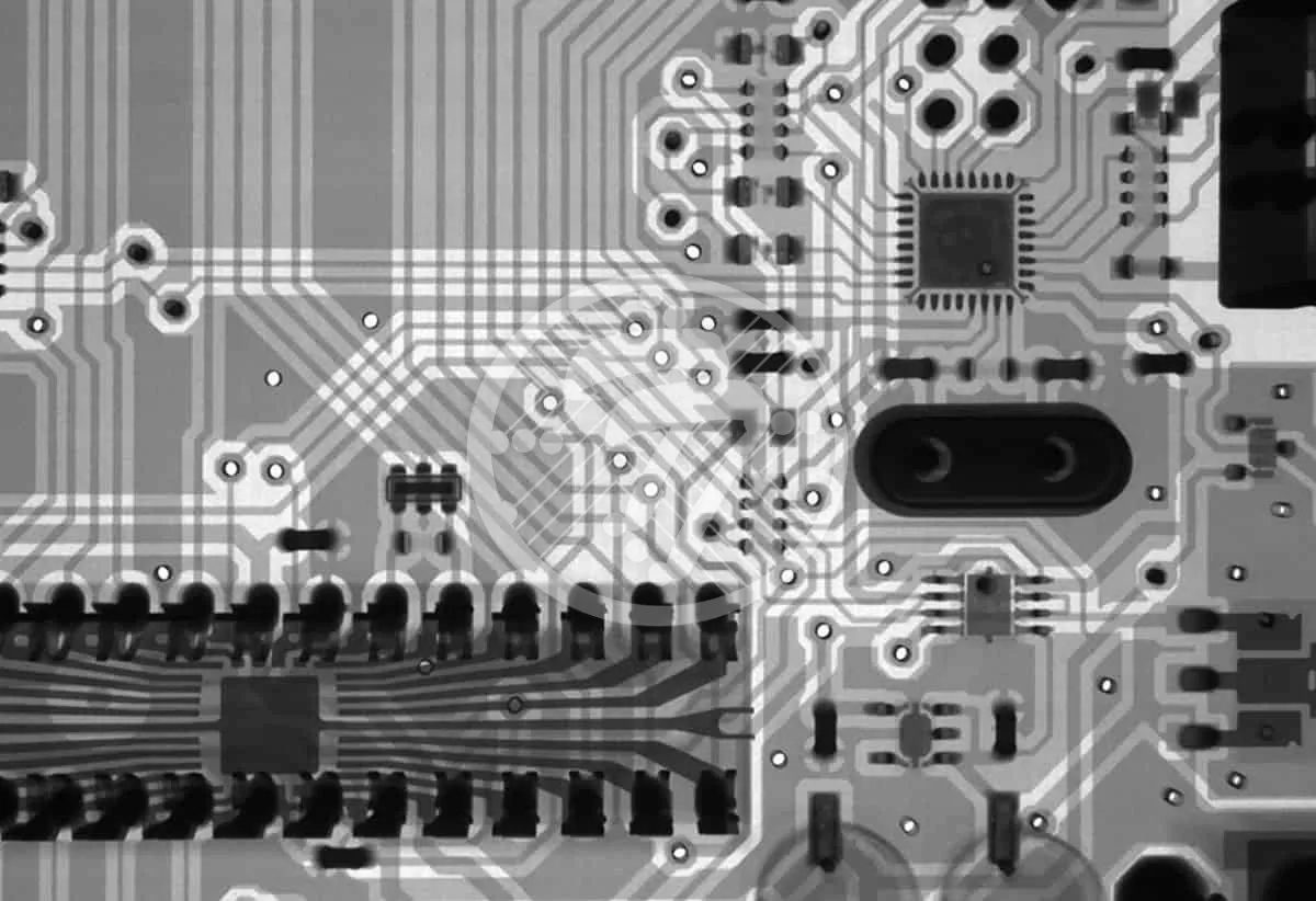
Technology Used in PCB –
Assembly process may use Surface Mount or Through Hole Technology. Sometimes though some assemblies may require both these technologies to be used, adding to the cost.
-
Single or Double Sided board –
A Single sided board assembly cost would typically be lower than one where you use a double sided board.
-
Number of placements –
Costs can typically increase with the number of placements required
-
Size of PCB components –
Typically smaller components and densely packed assembly boards add to the cost.
-
Availability of components –
It stands to reason that cost is also impacted by the (non)availability of components.
-
Compliance –
Often times testing to ensure assembly compliance also adds to the cost. Compliance such as RoHS and non- RoHS, IPC-A-610D Class I, II or III ITAR are often required, adding to the cost.
-
PCB Assembly Process needs –
Some PCB Assemblies could need a host of processes such as:
- Wave Solder
- X-Ray
- Automated Optical Inspection
- Hand Solder, and other such processes. These could add to the cost significantly.
-
Flexible or rigid PCB Assembly –
Typically flexible PCB Assembly cost is higher than that of a rigid one.
-
Coating –
Cost is also impacted by the coating requirements. Aspects such as whether you are using spray or a brush, the number of coats required, impact the cost.
-
Testing –
From thermal cycling to in circuit tests, there are a number of tests required before the PCB can be shipped. The testing in turn have a direct correlation with costs.
-
Flexible or rigid PCB Assembly –
Whether you need special containers or electrostatic discharge bags, once again can add to the costs
-
Delivery –
In case express delivery is required, costs are likely to increase.
Top tips to be kept in mind so that PCB manufacturing can be kept under check:
-
Look for multiple component sources –
This will help you to source components at the lowest cost without sacrificing efficiency. It will help to set up a process between the design engineering and purchase departments in order to ensure that conflicting priorities do not lead to a lack of cost optimization. Setting up cost reduction committees for example, could go a long way in identifying opportunities for cost reduction without of course negatively impacting efficiency.
-
Ensure that you do a Design-for-Manufacturing test –
This will take into account multiple factors at the design stage itself. Optimizing the bare board schematic will mean checking for areas such as:
- Complexity
- Number of holes and their size
- Via tech
- Material
- Layer Count
-
Prepare a complete BOM –
Simply put, the PCB bill of materials (BOM) as it is popularly called,is a list of parts and components used on the PCB. A complete Bill of Materials including details such as part number, manufacturer name, quantity, description, component replacements etc. can significantly expedite the quotation process, as also help source components at the right price. A thoroughly prepared BOM means lesser time spent back and forth and therefore greater efficiency.
-
Order Value and lead time –
Costs are typically inversely proportional to order value and lead time. Planning well in advance so that you can request for quantities at one go as also ensuring that you have enough lead time will help in controlling costs.
-
Inspection –
Even though testing and inspection adds to the cost, skimping on the same can have larger repercussions. Some manufacturers can offer in house inspection which can save you the time and hassle of getting a third party to inspect the boards.
Technotronix offers professional PCB Assembly services with 40 years of expertise. Our accurate PCB assembly process meets the quality standards, including ISO-9001:2015, RoHS, and more. You can rely on our PCB design tools that, in turn, lead to that perfect PCB Assembly. Our superior engineering capabilities mean that each board matches your exact requirements and technical specifications. If you have any questions or any requirements related to PCB assembly service, please feel free to contact us via email at sales@technotronix.us or call at 714/630-9200.