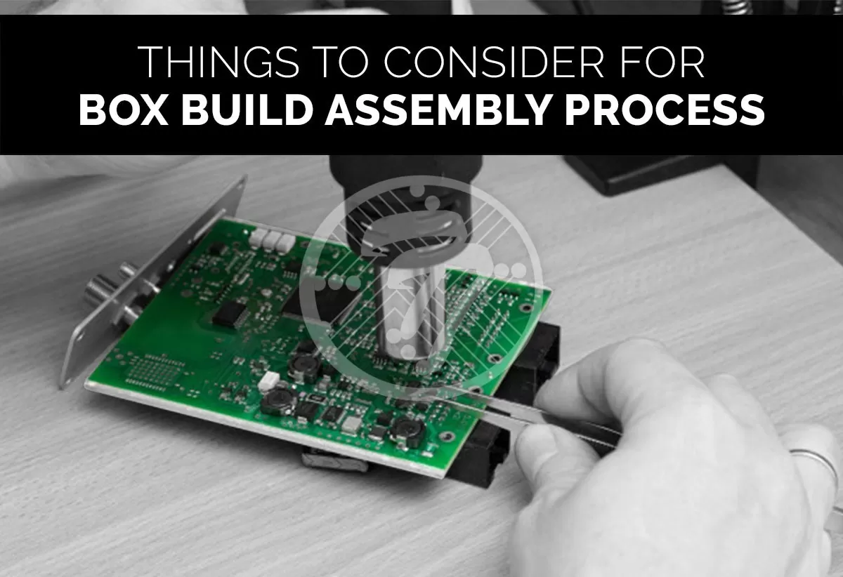
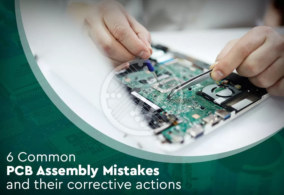
Turnkey PCB Assembly – A Comprehensive approach to get instant PCB quote and production

By | Date posted: | Last updated: November 11, 2022
PCB Assembly

The traditional approach to PCB assembly is riddled with many problems, foremost among them being the fact that it is high on cost besides being a long-drawn process. Also it typically supports large orders and isn’t suited for prototypes. Turnkey PCB Assembly therefore comes in handy as it serves as an antidote to all these issues faced with traditional PCB Assembly.

Essentially Turnkey PCB Assembly leverages cloud based software and makes the process of developing printed circuit boards hassle free. All you need to do is to upload a design. With Turnkey Assembly Services then the vendor deals with the entire assembly process including material procurement, PCB fabrication and assembly, testing, packaging and fulfillment.

Also checkout : PCB Assembly Service Quotes

Some of the advantages of Turnkey PCB Assembly include:

Prototyping

While traditionally creating a prototype is a lengthy process that involves dealing with multiple vendors, sometimes contending with out-of-stock-components and overall large lead times, Turnkey PCB Assembly allows for quick prototyping which in turn significantly reduces the time-to market. Needless to mention that it is a major source of competitive advantage.

Works for small orders

Traditional PCB Assemblies cater to large order batches and therefore aren’t conducive to prototypes as well as small orders. Turnkey PCB Assembly on the other hand, by virtue of being able to combine several small orders into a large run, can cater to any order quantity with ease. Irrespective of your order size you can therefore get exemplary service which otherwise can be a prerogative of large quantity orders alone.

Shorter Development Cycle

Turnkey assembly has a much shorter development cycle than traditional PCB fabrication, which in turn means that the PCB’s cycle from assembly line to market is much shorter. This is largely on account of the fact that time isn’t lost switching from phase to phase. Time saving is also on account of the fact that you deal with one vendor for your end-to-end requirement. With a shorter development cycle you tend to gain significant advantages when it comes to proactively responding to changing customer preferences.

No need to deal with multiple vendors

Turnkey PCB Assembly takes away the need to deal with multiple vendors, thereby reducing chances of miscommunication. With multiple vendors you often also face the issue of any delay causing a ripple effect. Also in case you need to make any changes, you need to find the right person who can execute it. It helps to have a single point of contact who can answer questions and implement any changes. Not to mention the fact that with one vendor assembling your final product, peace of mind is a given!

End-to-end services

Turnkey PCB Assembly typically offers end-to end services comprising of product assembly, inventory and shipping. This offers a number of advantages. Besides the logistical ease of a having one point contact, it also saves time as there are no cascading delays.

Perfect for small businesses

On account of the fact that Turnkey PCB Assembly can offer limited quantities as well as quick turnaround time, it works well particularly for startups and small businesses.  With professional prototypes delivered in short time spans, it becomes far easier to pitch the idea to investors as startups have an effective proof of concept to showcase.

Turnkey PCB Assembly also works well for Kickstarter creators who aren’t sure of the volumes they would require and hence cannot commit to large numbers at one go. The flexibility in quantity offered by turnkey assembly services also work well for hobbyists who want to experiment with ideas. Besides being a boon to small organizations, they can also work well for larger set ups that are nimble.

Identifies Problems Early

A major advantage of Turnkey PCB Assembly is also that it can identify any manufacturing problems early on. The manufacturer can identify any errors in design that can be corrected early thus saving the manufacturer from paying a heavy cost on account of design issues. In turn, it also helps establish better design practices in the long run.

Consistency

With Turnkey PCB assembly, consistency of results is a given thereby ensuring stringent quality standards. The importance of quality cannot be overemphasized in today’s competitive environment where a single inconsistency can lead to loss of reputation especially with social media on an overdrive.

From Concept to Delivery

With PCB fabrication, procurement, assembly, testing, packaging etc being taken care by the manufacturer, it eliminates a whole lot of stress while the vendor takes care of everything. You can therefore focus on perfecting your design and bring high quality products to life, far faster. Essentially then, with turnkey services there is a significant freeing of time for your team, which can in turn be used in other areas that need the manufacturer’s attention.

At Technotronix, we have over 4 decades of experience in offering high-quality custom boards. Our state-of-the-art machinery and experienced manpower can offer you products that are way ahead of the curve. Additionally, we have a huge vendor network when it comes to sourcing components. What that means for you, is that we offer you high quality products with a quick turnaround time and at optimal costs. A range of clients across industries have gained a competitive edge with our turn key PCB Assembly, California with our consistent delivery of high-quality, on-time, price-competitive products. To know more, please explore our PCB Turnkey Solution!

ATE PCB Assembly – The trusted interface between PCB manufacturer and OEM

By | Date posted: | Last updated: April 19, 2023
PCB Assembly

ATE (or an automatic test equipment) PCB is an important interface when it comes to verifying a semiconductor chip’s functionality. With semiconductor chip technology having become extremely advanced, testing the devices is a must do in order to verify its functionality and reliability. For the same reason it has evolved as a trusted interface between PCB manufacturers and their OEMs as it helps manufacturers to demonstrate the reliability of their products and for OEMs to believe in it.

ATE PCBs can test a wide array of semiconductor chips including but not limited to Microprocessors, field programmable gate arrays or FPGAs as they are popularly known as and many others. An ATE PCB however is designed to test a particular kind of chip set. Visit the link to know about Technotronix’s PCB Functional Testing Services.

Setting up of an ATE PCB Assembly

The setting up of an ATE PCB assembly requires superior technical know how as any hitch in the assembly can lead to lost time to market and therefore can have huge monetary repercussions. Since ATE PCBs differ from regular PCBs, ATE PCB managers must be well equipped with all the information regarding them. What they should also know is all the diagrams and illustrations that are associated with ATE PCBs. Additionally they must have thorough knowledge of the hardware as well as the PCB assembly process. Other than manpower equipped with technical knowledge, what is of essence is also an accurate ATE PCB pick and place system. What is also required is proper thermal profiling as also a solder sample, stencil design as well as an aqueous cleaning process. The ATE PCB pick and place system needs to be capable of handling large footprint boards. In addition the advanced versions also have features such as fine pitch repeatability and a large reflow oven. Another differentiating feature of an ATE PCB pick and place machine is selective soldering that ensures that through-hole components are perfectly soldered.

Thermal Profile

Every ATE PCB has a unique thermal profile. ATE PCBs are also known for their number of layers. While a network PCB has up to 20 layers, in case of an ATE PCB the number of layers could be as much as 60. On account of a number of power and ground planes, an ATE PCB also needs a large amount of heat in the reflow process.

The board therefore needs a specific thermal profile, which is characterized by high temperatures compared to a regular PCB. The temperature needs to be such that it heats up the board and yet does not damage the components. The first three zones are set at a higher temperature on account of the ATE PCB’s thickness. This in turn leads to a high ramp rate. Similarly, since it takes time for the paste to melt, the soak times are also different compared to a regular PCB.

Solder Sample

In order to arrive at the right thermal profile, a solder sample from the OEM is a must have. While in a regular PCB a profile can be created using the process engineer’s experience, however in case of ATE boards since no risk can be taken, a perfect thermal profile is created using the solder sample. Only when the perfect thermal profile is created, is the live product run through it.

Stencil Design

Another necessary step that ensures that the solder paste is dispensed properly is a stencil design. Stencil apertures impact solder reflow behavior and are therefore if not used correctly, they can adversely impact the assembly process. Tombstone and bridging is often the result of an inaccurate stencil design that can lead to a whole lot of costly re-work. In turn this causes delays in shipping, increased cost, increased time-to-market, not to mention the stress on the other components of the board.

DUT

An important aspect of ATE PCB is its device-under-test site. Any compromise on the part of the DUT can result in the ATE PCB being compromised. For example, if the nuts that are used to keep the DUT socket in place are not properly installed, the DUT socket will not be correctly installed and testing will not be possible. Also DUT pads are sensitive to any contamination. It is therefore important to use solder less pins.

Cleaning

Proper cleaning of the ATE PCBs is a significant requirement as any residue can impact the speed of the board. Any foreign particles or even a fingerprint can jeopardize the efficiency of the board. What is required, therefore, is aqueous cleaning so that all the residue is cleaned from the board using special chemicals.

While ATE PCB assembly is a trusted interface, what it needs is a high degree of maintenance for it to operate at its optimum level and offer the degree of accuracy required.

TechnoTronix is a leading manufacturer of high quality ATE PCB assembly service to electronics manufacturers. Our qualified team of professionals uses the modular approach for PCB Assembly and Layout to simplify the complexity for the Internet of Things Applications. Check out our PCB assembly services! Also, you can drop an email to sales@technotronix.us or give us a call at 714/630-9200 to solve your queries or to get a quote.

Why Ball Grid Array (BGA) is important in PCB assembly?

By | Date posted: | Last updated: December 13, 2022
pcb-assembly-2

The importance of the right pcb layout cannot be overemphasized. While it connects various electronic components on a single substrate, it is the method by which components are attached to the board’s surface that can go a long way in affecting its stability as also its efficiency.

A Pin-grid array, popularly referred to as PGA, was by far the standard in packaging integrated circuits on a board. The same, however, has now been replaced by the Ball Grid Array or BGA. Simply put, while the PGA used a square arrangement of pins to mount components, BGA replaces pins with metal balls made of solder attached to the underside of the unit.

A typical integrated circuit designed with BGA comprises of a chip or processor that is attached to the substrate. The die in turn is connected to the slab through a wire. Solder balls are then attached to the other side of the substrate. The ready component is now referred to as a package. The package then is fastened to a circuit board by way of the use of solder.

Also checkout: What is BGA Reballing? Why does Ball Grid Array require Reballing?

There are several advantages of Ball Grid Array (BGA), primary among them being:

  • Lower track density

    – With metallic solder balls arranged in a grid like pattern. Track densities can be significantly reduced. In turn what it means is an optimized pcb layout as the closeness of balls increases the efficiency. Trying to do the same with a Pin Grid Array, by increasing the volume of pins enhances the risk of accidental bridging. In case of BGA, however, with the balls made of solder, bridging isn’t that much of a concern.

  • Reduced chances of component damage

    – A pin grid array requires a soldering process that has chances of damaging the component. On the other hand, with BGA, the solder balls only need to be heated so that they melt and adhere to the PCB. The chances of any component damage, is therefore significantly reduced. Also, the surface tension between the ball and the circuit board ensure that the package is held in place.

  • Reliability

    – With the use of PGA, the fragility of the pins was always an issue. They require extreme care and are prone to being bent and damaged. With BGA using solder pads connected to solder balls, the system is far more robust and reliable

  • Improved performance

    – On account of the grid array the connections inside the BGA are shorter. What it translates into is reduction of lead induction level leading to improved performance typically at higher speeds.

  • Lower incidence of overheating

    – Reduced heat resistance between the BGA and the circuit board offer a major advantage. In fact, the heat generated dissipates into the circuit board as the BGA units provide thermal channels to direct the heat away

This however, is not to suggest that the ball grid array does not come with its own set of issues. Primary among them, being the inflexibility of the balls! In fact, the rigid bond between the board and the component can result in physical stress, which in turn can impact efficiency. Also on account of the proximity between the board and its components, it can be quite a task to make a thorough check of the quality aspects of the PCB. Also, it is not easy to rework boards that contain BGAs unless the correct equipment is available. A faulty BGA will therefore need to be removed by locally melting the device. Great care is needed to see that other devices in the vicinity aren’t affected or damaged. Once removed, of course the BGA can be replaced with a new one.

There could therefore be a number of applications where BGA isn’t the best alternative. In such cases a variation of the standard BGA, called PBGA or Plastic Ball Grid Array is used. It has a plastic-coated body, a substrate that is glass mixture laminated and has copper traces. What it does for the system is that it displays increased stability as far as temperature is concerned. Also, it uses pre-formed solder balls that can be reshaped. There are also a whole lot of other BGA types that can be used in different situations.

Important among BGA types them are

  • Moulded Array Process Ball Grid Array or what is called MAPBGA, this is ideal for low to mid performance devices that comes at a low cost.
  • Thermally Enhanced Plastic Ball Grid Array or TEPBGA, this package provides for high heat dissipation levels.
  • Tape Ball Grid Array or TBGA, this is ideal for mid to high-end solutions.
  • Package on Package or PoP, this allows for stacking a memory package on top of a base device and hence is useful for applications where space is a real constraint.

Technotronix offers professional PCB Assembly services with 40 years of expertise. Our accurate PCB assembly process meets the quality standards, including ISO-9001:2015, RoHS, and more. You can rely on our PCB design tools that, in turn, lead to that perfect PCB Assembly. Our superior engineering capabilities mean that each board matches your exact requirements and technical specifications. If you have any questions or any requirements related to PCB assembly service, please feel free to contact us via email at sales@technotronix.us or call at 714/630-9200.

Simple Ways To Reduce PCB Assembly Cost

By | Date posted: | Last updated: February 14, 2022
pcb-assembly1

When it comes to high cost being a common crunch regardless of the improving economy, many of the American industries are tracking down the effective ways to scale back the costs and upgrade profit margins without compromising on quality aspects of product and process development especially in the electronic industry. One of the most trending issues experienced by electronic manufacturers and OEM is constantly changing technology with the need of more and more complex PCB assembly services. For all these issues, there is certainly a happy medium or a middle ground to be considered to reduce the cost of PCB assembly with maintaining the quality standards in every phase of the PCBA. So folks! Let’s rev up to further content that uncovers savvy ways for making the PCB more cost effective with smart steps to bringing modification to the assemblage of printed circuit boards.

It’s all about keeping it pretty simple, easy and as direct as possible to reduce the cost of PCBA instead of seen it as a complicated dance to make it more compact, multi feature and reliable. For most of the electronic manufacturers, searching for the zone that proves vital for safely minimizing the spending along with keeping the customers satisfied with the quality products isn’t easy. It’s difficult to balance the project schedule and budget at the same time. On the other hand is the strict inspection operation that drives an increase in cost which proves more expensive if ignored or not implemented during a PCB assembly. With this, why not gain more fortunes of cost savings by trying out some simple ways and method?

Top PCB Assembly Cost Breakdown ways

  • Minimize complexities

    by coming up with many different design options that can help to plan out suitable prototype at a first go.

  • Shape it right

    by applying a common structure to cut down on the cost. Complex shapes usually result in a cost rise.

  • Smart and Slick pcb layout

    are at the rim of the basket. One of the significant stages in PCB assembly that steals the show along with a need of effective planning to curtail the cost is the pcb layout phase. The optimum use of required high quality parts and components that can promptly lower down on the cost per PCB is possible with strategical PCB engineering.

  • Take sufficient time to come up with a complete and categorical Bills of Materials (BOM). An effective BOM should include all the essential elements like reference designator, part number, description, quality, SMT method, manufacturer name, footprints, package and BOM level. It is of utmost consideration to add the

    element of Component Replacement in the BOM

    as the technology develops faster and need the old elements to be immediately be replaced with the new ones to match up the competitive market trends.

  • Avoid extra cut outs in the boards

    that can add on to the cost of PCBA that doesn’t make a vital difference on brand recognition or functionality.

  • Go ahead with a

    strict DFM check

    to probe for a particular circuit is normally implemented that can taper off the cost of PCB assembly.

  • Plug in to the chief factors considered or headway to perfection with effective optimization and revamp

    the schematic layout of a bare PCB.

    Simply get a basic idea of the factors presented in the following diagram: (Insert the image)

  • Work out a good deal with a

    fine balance of order value.

    More the order, lesser the price of each PCB assembly.

  • Adjust the lead time

    after knowing the way your PCB assembler calculates the lead time. Clear all your doubts pertaining to the initiation of the start time, day of order, day of payment, date of receiving the components, etc.

  • To

    consciously choose a professional expert

    and reliable PCB manufacturer/ PCB assembler. The majority of the PCB assembler declares to offer cost effective PCB assembly services. But many customers don’t get satisfaction since they do not receive what is being claimed.

To avoid these kinds of vital issues, Let’s take a jaunt to factors that will help to choose your PCB manufacturer very consciously:

  • Look for the Certifications

    that assure a good manufacturing capability and quality management system of a PCB assembly service. RoHS compliance, ISO9001, UL and many more are the international quality management standards that have now become mandatory to improvise the quality of process and products.

  • High-tech equipments,

    well defined tool room and implementation of upgraded technology contributes to receiving quick turnarounds along with high efficiency, required manufacturing speed, high precision placing and effective inspection. In the present world of innovation, with the adoption of Surface Mount Technology, Through Hole Technique and other specialized PCB technology, these factors need to be of prime priority in the checklist.

  • Component procurement

    is also one of the chief considerations for selecting a suitable PCB manufacturer. Apart from focusing on the PCB engineering and PCB fabrication mechanism, it is of great concern to verify the component sourcing capabilities, vendor management and supply chain network that are competitive at large.

At Technotronix, we are fully equipped to handle your PCB manufacturing requirements. With over 4 decades of experience in PCB manufacturing as well as assembling PCBs with differing levels of complexities, we follow industry best practices to ensure we deliver cutting-edge products. Our team of experts and state-of-the-art equipment ensures that all our PCBs meet the industry standards of quality and testing. It is our vast portfolio of satisfied clients that stand as the biggest testimony to our success. In case if you have any questions, please feel free to contact us via email at sales@technotronix.us