The Complete Guide on PCB Milling in Circuit Board Fabrication!

By | Date posted: | Last updated: November 30, 2021
PCB Milling

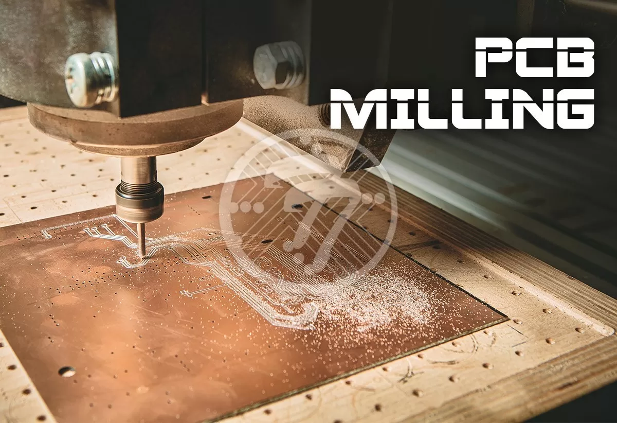
PCB Milling also sometimes referred to as isolation milling or seclusion milling is an important process that is required to ensure high quality PCB boards.

Simply put, PCB milling is an eliminative process that involves the removal of copper tracts from the PCB substance. This ensures that pads are reproduced and configurations established on the PCB design. While milling is similar to etching, in that both are eliminative processes, milling, unlike etching does not involve the use of any harmful chemicals. It is therefore an ideal choice for anyone without a proper lab environment for etching. Also, etching chemicals are usually corrosive and produce harmful fumes when they react with copper traces.

Advantages of PCB Milling

PCB Milling offers a number of advantages when it comes to prototyping as well as some special PCB designs. The biggest advantage, of course, is that it does not involve the use of harmful chemicals. With etching of course not only do you need proper chemical handling but also a proper disposal method in place. The wet process is also unsuitable for high resolution boards.

With a CNC PCB milling machine you can create quick PCB prototypes without worrying about the chemicals. Also the CNC machine can undertake both drilling as well as milling and in some cases also the cutting.

It is important to remember, however, that both milling and etching are preferred under different circumstances. If the requirement is for mass production, for instance, etching is preferred.

PCB Milling Design Parameters

Below is a detailed guide on the design parameters involved in PCB Milling:

  • The regular diameter of the PCB mill device is 2 mm while
  • the lowest diameter is 0.8 mm.
  • The internal or external silhouette of the PCB can be milled as per requirements.
  • The borders of the rectangle need to be circular. It is also important that the connected milled area is pierced at every intersection.
  • The skeleton and separations of the PCB are milled as in its absence the strength of the PCB board may be impacted. Also, the internal and external silhouette of the PCB board needs to have a layer width of 1 micrometer.

PCB milling process

It essentially involves two systems, namely the hardware and software systems.

Software system

There are two types of software:

  • Raster
  • Vector

Raster typically does not have high resolving power as compared to Vector.

Hardware system

The hardware system is the numerically controlled milling machine. The system has either a serial or a parallel port that is connected to the main controller. On receiving the signals, the controller drives the positioning system which adjusts the milling head speed.

The movement around the X/Y axis is controlled by stepper motors. The Z-axis drive is also powered by a non-monitored lead screw.

Tips for CNC PCB Milling

Some of the tips to ensure effective printed circuit board milling include:

Leveling

This is crucial as you need to ensure that a uniform level is achieved when subtracting the metal layer off the board. Leveling can be achieved in two ways, physical leveling and computer leveling. Physical Leveling is done using a floating head CNC machine. The milling tool is maintained at a fixed distance from the board. Computer Leveling offers yet another possibility of achieving a uniformly milled PCB. In this leveling, the distance from the board is adjusted through a software.

Track clearance

It is important to pay due attention to the track clearance. Typically a 0.5 mm track clearance is used.

G-Code files

If you are using a machine that can undertake cutting, drilling as well as milling, it is important to have a G-code file for every operation

Coating

It is important to apply a solder mask as once milled the exposed copper can erode.

Safety

When drilling fiberglass you will be subject to dust. It is important that the dust isn’t inhaled. For this purpose, a vacuum cleaner should be used. You can also avoid this issue by using non-dusty FR1 and FR2 copper clad boards.

To sum up

PCB Milling offers a cost effective solution to make strong boards. It is imperative however to follow these tips to ensure that the process is effective.

Technotronix is one of the leading PCB manufacturers based in the USA. We have adopted advanced methods and technologies, which can give you the finest PCB fabrication services. We are adhering to strict high-quality standards and compliant with the RoHS (Restrictions of Hazardous Substance) directives.

If you have questions or queries related to any kind of PCB manufacturing services, email us at [email protected] or call us on 714/630-9200.

Top EMI and RF Shielding Methods for Custom Flexible PCB!

By | Date posted: | Last updated: November 11, 2022
custom-flexible-pcb

Custom Flex PCBs are subject to both Electromagnetic as well as Radio Frequency Interference. In turn, this can lead to a whole lot of consequences including but not limited to an increase in error rates.

To protect custom flexible PCBs against this interference, it is important to carry out EMI shielding. This can be done by way of copper layers, silver ink and shielding films, each of which comes with a distinct set of advantages and disadvantages.

Let us look at the process in some detail as also look at the selection parameters:

What is EMI and RF shielding?

It is a method that prevents electromagnetic and radio frequency interference from external signals.

In addition, it prevents high-frequency signals from leaking out. This is done by using metallic barriers. Essentially the shielding effect is based on a principle used in Faraday Cage, which is that the metallic screen surrounds the sensitive or transmitting electronics.

In selecting the type of EMI shielding, it important to consider the following two aspects, namely the bend requirements and the controlled impedance.

Bend requirements

The minimum bend capacity is a function of the thickness. It can, therefore, reduce the bending capacity of the PCB. It is important, therefore, to evaluate the minimum bend radius and bend type requirements for shielded designs. Another aspect to consider includes whether the bend required is static or dynamic. It is important to remember that the bending capacity of a dynamic flex circuit board is far higher than that of a static one.

Controlled impedance

In Flexible PCB Board, the controlled impedance signal requirements also impact the EMI & RF shielding approach. The shields need to have electrical properties that meet the necessary criteria to obtain the appropriate impedance values.

Types of EMI & RF shielding used in Custom Flexible PCB

EMI shielding is done using 3 types of materials, namely:

  • Copper Layers
  • Silver Ink
  • Shielding Films

In making the choice of material, some of the considerations include:

  • Shielding Performance
  • Mechanical Bend Capabilities
  • Suitability for controlled impedance

Copper Layers

Here the copper layers are used either as solid or cross-hatched planes. They are linked to the ground through stretched vias. The solid copper layers tend to provide a higher degree of shielding. Cross-hatched layers, on the other hand, are used where shielding is required without impacting the board flexibility.

The disadvantage of this shielding, stems from the fact that it increases the thickness which in turn affects the bending capacity. In fact a three-layer copper shielded flex circuit increases the thickness by nearly 125%.

Also, the fact that the shielding layers are connected to the ground plane through vias, tends to act as a mechanical stress concentrator.

Silver ink

As opposed to copper layers, silver ink has the advantage of offering greater flexibility at a lower cost. A silver ink shielded flex circuit is only about 75% thicker. Additionally, silver ink uses selected perforations in the coverlay. These perforations, in turn, allow for electrical interconnections.

Also, silver ink is relatively inexpensive as compared to other shielding material.

Specialized shielding films

These are suitable for dynamic bend applications and are suited for small structures. These also work well in sensitive applications.

Essentially it involves an electrically conductive adhesive, a metallic layer, and an insulating layer to be laminated. It is then bonded on the surface of the coverlay.

In terms of thickness, a 2-sided shielded film is only 15-20% thicker.

What are some of the design tips to avoid EM and RF interference in Custom Flexible PCB Boards?

  • Sharp bends need to be avoided as they lead to fluctuations in impedance and signal reflections.
  • It is important to isolate high-speed and low-speed signals.
  • It is imperative that the current return path be kept small
  • Vias should not be placed in differential pairs
  • If split ground planes are required, they should be connected at a single point

To sum up

To ensure that the shielding is reliable and cost-effective, it is important to undertake a thorough examination of all aspects of the electrical and mechanical design factors. This will help in arriving at the right shielding method that works well for your Flex PCB.

At Technotronix, we are fully equipped to handle your PCB manufacturing requirements. With state-of-the-art equipment, we deliver the highest quality boards that you can rely on. No matter how complex your requirement, you can count on us to deliver to your bespoke needs. Our stringent quality control processes ensure that the boards deliver to your benchmarks.

To get more insights into the PCB fabrication, multilayer PCB fabrication & quick turn PCB fabrication, please explore our PCB fabrication services. Also, you can drop an email to [email protected] to solve your queries or to get a quote for custom flexible circuit boards, rigid-flex PCBs, flexible printed circuit boards manufacturing, flexible PCB prototyping.

Rogers PCB Vs FR4 PCB – What is the Difference?

By | Date posted: | Last updated: February 14, 2022
rogers-pcb-vs-fr4-pcb-1

Introduction

In the world of hi-tech gadgets, medical equipment, and Industrial Machines, the performance of any product depends mainly on the quality of its PCB design.

Though there are multiple aspects to be considered while designing a PCB, our focus here is to identify the right PCB material which is also known as Substrate. Substrates are the di-electric sheets that hold the components and traces of a design. Selecting the right substrate material for a specific application is the key aspect of PCB design. To decide which substrate works best for any given application, we need to know the salient features of all the materials available on the market. The materials offered include FR1 to FR6, CEM1 to CEM5, insulated metal substrates, Polytetrafluorethylene (PTFE), polyimide, etc. Among all these, FR4 is considered the most commonly used substrate by many PCB manufacturers.

What makes ‘FR4 PCBs’ a commonly used type?

FR4 PCBs (Printed Circuit Boards) are widely used, low-cost PCBs categorized as ‘Best Performers’ in most environmental conditions. As per the NEMA standard, FR4 signifies the Fire-Retardant characteristic of the composite material. They are made from woven fiberglass cloth reinforced with epoxy resin. FR4 material is the most cost-effective type available for circuit board fabrication. They are lightweight, moisture-resistant, and have high dielectric strength.FR4 PCBs are an appropriate choice for through-hole technology in component mounting. Thus, they are extensively used in most manufacturing techniques and provide high yield.

Then why Rogers PCBs are required?

Roger PCBs are manufactured by Rogers Corporation and are mainly used in high-frequency and high-speed designs. Their excellent dielectric constant and ability to sustain elevated temperatures make them the Best Quality PCBs for RF products and microwave devices. They are available in several types based on required board resistance and high dielectric constant. Roger PCBs are good in thermal management and hence maintain the consistency of the product. Also, they have low outgassing, a vital feature necessary in the space and aeronautics industry.

So, let’s understand the Differences between Rogers PCBs and FR4 PCBs:

Cost is the first and foremost difference to be considered in this section. The ultimate goal of any PCB manufacturer is to bring out a cost-effective circuit board with the best performance. FR4 PCBs are the most affordable ones in the market. This is valid if your design is for optimal conditions with low-frequency and nominal temperature settings. If your application demands high speed or extreme temperature operations, then you may have to overlook the cost and go for expensive Rogers PCBs.

Impedance Stability is the next difference between FR4 and Rogers PCBs. The dielectric constant of the substrate is one significant factor that defines the Board Impedance and its stability. The higher the dielectric constant, the higher is the Impedance stability. Though FR4 is the cheapest substate available, its maximum di-electric value is 4.5. Whereas Roger PCBs has a higher and wider range of di-electric value like 6.5 to 11. This feature makes Rogers PCBs the best choice in high-thermal applications where the stable impedance is crucial.

Thermal Management is in continuation with the previous difference we have discussed. In high-speed applications, there will be significant heat generation in the PCB, and it must be handled diligently with a good thermal management system. In such scenarios, a thermostat-based laminate present in Rogers PCB is the best choice. FR4 PCBs cannot handle high temperatures and thus fail in such applications.

Dissipation Factor indicates the signal loss in the PCB which is much lower in Rogers PCB as compared to FR4 PCBs. The dissipation factor of FR4 PCBs is 0.02% as compared to 0.004% in Rogers PCB. So, Rogers PCB provides reliable results with minimal electrical signal loss against FR4 PCBs.

Moisture Absorption is directly related to the electrical and thermal characteristics of the substrate material. This in turn affects the performance of the circuit board. Rogers PCB has the least moisture absorption and thus provides the best efficiency in varying environmental conditions.

Applications and Performances Based on the overall performance, FR4 PCBs are considered as Decent players whereas Rogers PCBs are remarkable performers. Hence FR4 PCBs are best fit in the optimal environment with low to mid-frequency applications. They are robust and deliver excellent balance in electrical stability and are easily manufacturable in almost all existing processes in the PCB industry. Whereas Roger PCBs are meant for high-grade performances in niche domains like space applications. The temperature constancy and low outgassing feature make them the best choice for critical applications like space and aerodynamics.

Let’s conclude

Diverse applications in the electronic industry come with a demand for varied types of PCB requirements. Based on the usage and performance, it is necessary to make the right choice of PCB material that can bring out the best product to your customer. So, is it FR4 PCB or Rogers PCB?
The end application is the best selection criteria.

At Technotronix, we combine state-of-the-art technology with our advanced engineering to offer you Rogers printed circuit boards & FR4 Printed Circuit Boards of the highest quality. With over four decades of experience in delivering high quality, on-time, price-competitive products, you can rely on us for your PCB requirements.

To get more insights into the PCB fabrication and PCB assembly services, please explore our PCB fabrication services. Also, you can drop an email to [email protected] or give us a call at 714/630-9200 to solve your queries or to get a quote.

Single-Layer vs Multilayer Printed Circuit Boards: Who Wins the Ultimate Battle?

By | Date posted: | Last updated: April 19, 2023
multilayer-printed-circuit-boards

When it comes to choosing the right custom PCB boards for your project the one question that you need to deal with at the outset includes whether to go for a single-layer or multilayer printed circuit boards. How do you decide whether your project require single-layer or multilayer printed circuit boards? To be able to answer this question, it is important to get into a detailed understanding of both.

Single-layer or single sided PCBs

A single-sided board, as its name suggests has the components on one side of the board and the conductor pattern on the other. Typically, such boards are used for simpler devices.

Single-Layer PCB Advantages

The many advantages that single-layer printed circuit boards offer, include:

  • Low Cost
    The simpler nature of these boards translates into the fact that they need fewer resources, less time as also lesser expertise to design as well as fabricate the boards. All of this translates into low costs of single-sided boards rendering your project, efficient.
  • Easy to design and produce
    Because of their simplicity, it is easy to design these boards as also for manufacturers to produce them without any issues. Additionally, it is easy for manufacturers to cater to high volumes. In fact, with rising quantities, the price of the board will be even lower, making the boards even more efficient.
  • Quick turnaround times
    Once again the simplicity of the boards lend themselves to quick turnaround times even at high volumes. This can prove to be a significant source of competitive advantage as your go-to-market plan can be expedited.

Despite the many advantages that they offer, single-layer PCBs also run into several limitations, important among them being:

  • Limitations of design
    While the simplicity of their design is an advantage in several terms, it can also turn out to be their limitation. For complex devices where there are many components, the space offered by a single-layer printed circuit board does not prove to be enough.
  • Power and Speed
    With limited number of connections, the power and speed of the board is significantly impacted. This makes single-sided PCBs not too usable when it comes to complex devices where power and speed is of essence.

Single-Layer PCB Applications

Because of their low cost and ease of production, single-layer PCBs find a place in several devices were storing of a large amount of data is not a prerequisite. Some of the devices where single-layer PCBs find wide-spread application include:

  • Radios
  • Printers
  • LED lights
  • Calculators
  • Coffee makers
  • Sensors, and more

Multilayer Printed Circuit Boards

Multilayer PCBs are made up of three or more double-sided boards stacked together. With multiple conductors patterns the area available for wiring significantly increases. Typically, an even number of layers are preferred as odd number of layers can lead to issues such as warping and twisting once the soldering process is done.

Multilayer PCB Advantages

The many advantages that multilayer PCBs offer, include:

  • Useful for complex designs
    Complex devices that have a high number of components and circuits benefit from the use of multilayer PCB. Devices with several uses as well as advanced capabilities need this kind of complexity. With the miniaturization of devices becoming a growing trend, the use cases of multilayered PCBs are only rising. Many of the multilayered boards also come with features such as impedance control and electromagnetic interference shielding, further improving the quality of the board and of the device.
  • High on Power
    Because of their high circuit density, the boards are also more powerful. What this means is that they offer high operating capacity as well as speed, making them especially useful for advanced devices.
  • Highly Durable
    With an increased number of layers, the thicker board is also more durable. It is far more capable, therefore, of withstanding harsher conditions.
  • Size
    Small size and lightweight are added features of a multilayer board. This makes them ideal for the miniaturization of devices.
  • Single connection point
    The fact that they work with a single connection point is an added advantage in terms of simplicity of design and weight.

Also checkout : Advantages of Multilayer PCB in Electronic Industry

Limitations of Multilayer PCBs

Despite the many advantages that multilayer boards offer, the limitations that they present include:

  • Increased manufacturing costs
    As opposed to single-layer PCBs they come with a higher manufacturing cost.
  • Potentially longer manufacturing time
    Because of the complexity of design and high component density, typically they come with a longer Manufacturing time.
  • More complex repairs
    In terms of repairs too, the process is more complex as well as time consuming.

Common applications of Multilayer PCBs include:

  • Computer components
  • Mobile phones
  • GPS devices
  • Heart monitors
  • X ray equipment
  • GPS technology
  • Automotive industry
  • Aerospace industry
  • Military applications, and more.

Single-Layer vs Multilayer PCBs, who wins the ultimate battle?

The answer to that lies in your requirements. It is the project that will determine the type of board that works well. To come to the right conclusion on what kind of board will work well for you, you need to consider the following aspects:

  • The level of functionality required- More complex functions require multi layered boards.
  • The acceptable size- If your requirement is that of a smaller space, multilayer boards are likely to work better.
  • The need for durability- Typically multilayer PCBs are more durable.
  • Your budget- If your budgets are low, single-layer PCBs are likely to make a better fit.
  • Timelines- Single-layer boards have faster turnaround times.

So go ahead and make the right choice!

At Technotronix, our highly qualified and experienced multilayer PCB manufacturer ensure that all the layers are correctly registered. Adhering to high quality multilayer PCB manufacturing practices, we are equipped to handle complex boards with up to 24 layers, which are laminated to insulate them. Whether it is sticking to the product specifications or stringent quality controls, there is no stone that we leave unturned in our quest to deliver the best.

Get a Quick PCB Fabrication Quote