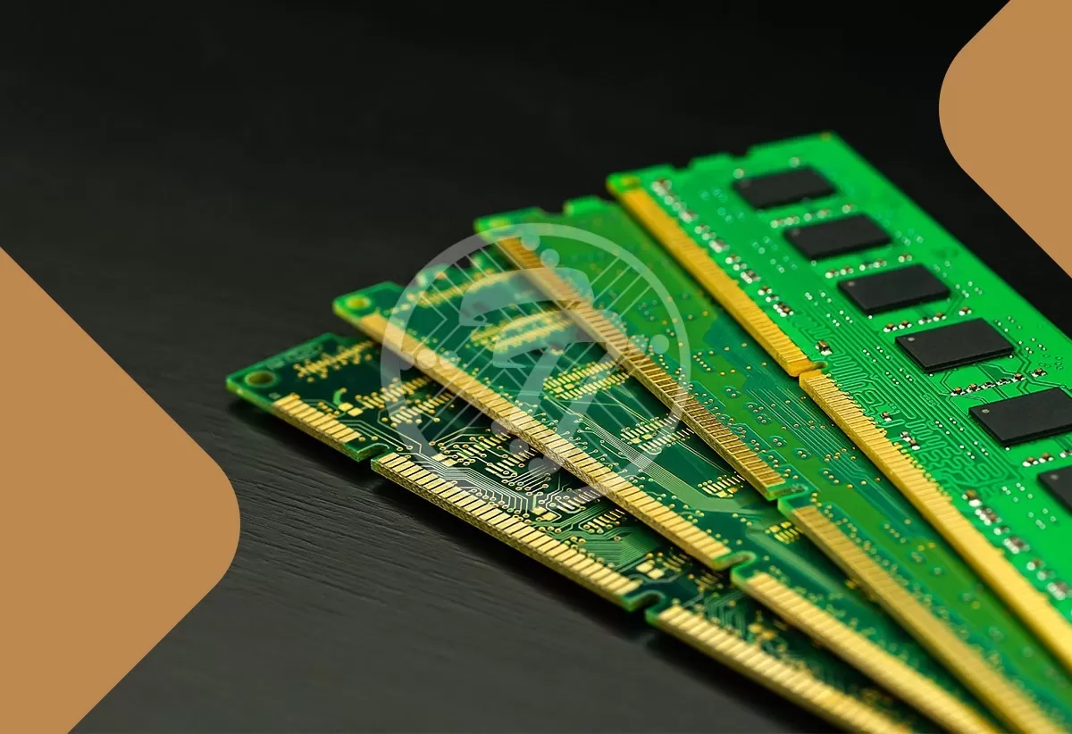
RF/Microwave PCB Play the most important Role in High-Speed PCB Design!


What is your knowledge about RF and Microwave circuits? If nothing, then you are at the right place to understand everything about RF and microwave circuits. A few decades ago, no one was familiar with the word RF and microwave circuits because of their complex design in manufacturing these circuits.
The technology was not that advanced, simplifying circuit making, creating complexity in manufacturing RF and microwave PCBs. But in the current era, RF and microwave circuits are becoming a very crucial part of industrialization. RF circuitry is getting crammed into a wide array of commercial products. With RF circuitry, manufacturers are preparing wireless devices for several Industries like defense, medical, and communication applications, making RF circuits a crucial part of businesses. Check out top design guidelines for RF and Microwave PCB Assembly!
Not just RF circuits, but microwave circuitry can capture very high frequency (VHF) and Ultra high frequency (UHF) to the circuit. Now high-speed PCBs are getting RF and microwave technology to enhance the operational quality of the PCB. RF and microwave circuits have surpassed several challenges that the PCB manufacturers were facing previously, and now PCB manufacturing is becoming accessible for preparing RF And Microwave Printed Circuit Boards.
The range of RF Technology varies from 500 MHz to 2 GHz. After 2 GHz, the PCB designs come into the range of Microwave Printed Circuit Boards. So now we can differentiate between RF and microwave circuits, which are digital or analog.
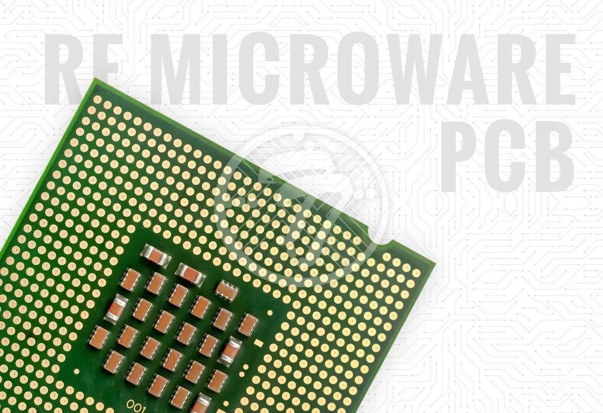
What is an RF PCB?
Generally, PCB industries consider 100 MHz circuit boards as an RF circuit, which is quite understandable. The frequency range of RF circuits is very high, creating ample PCB solutions in manufacturing and operations.
Industries are widely using RF circuit boards to successfully operate their business and find smart solutions after completing the circuit board design.
What is A Microwave PCB?
Microwave PCBs are the most used Printed Circuit Boards whose radio frequencies are above 2 GHz. This means these circuit boards can be operated only on high frequencies. Most communication signals and applications use Microwave or RF circuit boards, and these are the fastest PCB manufacturing technology.
Why Do Industries Need Microwave PCB and RF PCB?
For preparing fastest printed board circuits, manufacturers can commonly use Microwave printed circuit boards and RF circuit boards to transmit fast radio signals. Our boards have many different applications like wireless technologies, smartphones, robotics, security, and sensors. This means RF printed circuit boards are becoming a crucial part of modern industries.
If you think of preparing a fast-printed circuit board that can transmit millions of signals in minimum seconds, then RF circuit boards can help you get the finest solutions. Similarly, Microwave printed circuit boards can hold more frequencies than RF circuits, which means they can handle billions of communication signals in a couple of seconds.
Radio Frequency printed circuit boards are high frequency printed circuit boards that can enhance electronic appliances’ performance and their applications in the industries. With this instant application, these printed circuit boards are commonly used by defense, electronics Industries, smartphone industries, and other top industries that need printed circuit boards for a smooth operation.
RF and Microwave printed circuit boards are crucial to enhance each other’s performance, commonly used in aerospace sectors. Just because of the negligible errors in RF and Microwave printed circuit boards, industries are widely using these circuit boards to get a high-performance aerospace application.
Nowadays, digital signals are crucial in every circuit, and it is creating a fast transmission path for signal transformation. Also, RF PCBs and microwave PCBs can maintain dielectric constant, thermal conductivity, thermal coefficient of dielectric constant, and thermal expansion coefficient.
What are the factors affecting RF PCB & Microwave Printed circuit Boards?
Preparation of Microwave circuit boards and RF circuit boards are still difficult for manufacturers. Due to it, manufacturers face some problems in transmitting the radio signals and also have tight impedance tolerance.
If we talk about old age PCBs, radio and microwave signals are sensitive to noise, and they can respond directly to it. It can affect the quality of printed circuit boards, and also, manufacturers did not manage ample RF and Microwave printed circuit boards to get the perfect shape.
It affected these printed circuit boards’ operational quality and created complexity in transmitting radio signals to the printed circuit boards. Nowadays, industries are using high-speed printed circuit boards to operate several operations in the company. Some of these factors like impedance mismatch, size grounding, arrangement, and Kelvin connection can affect RF’s speed circuit boards.
RF circuit boards are giving multi gigahertz speed to the transmission of signal, and they can absorb energy in the form of heat. The signal transmitting on the circuit boards is fast, which is giving fast operations to the companies. Manufacturers are managing these printed circuit boards by reducing the resistance in cross-section for higher heat loss.
Conclusion
We are the top high-speed PCB manufacture in USA who gives you the fastest transmission speed in Microwave printed circuit boards. With this quality, you can find cost-effective and thermal effective printed circuit boards with ultimate durability.
Several factors can affect the durability of printed circuit boards, like the environment, which needs to be fixed on time. Our experts find smart solutions using the latest technologies available and prepare the best PCB prototype for Microwave printed circuit boards and RF circuit boards. It can enhance the operational qualities of your devices and will enhance the speed of signal transmission.
The experts understand every needs of industries, and prepare the best high-speed PCB design to utilize its speed to the end result. Mixed signal PCBs have complex designs, which have several complications while manufacturing. Our experts use the latest technical tools to prepare every Radio Frequency Printed Circuit Board.
The performance of these PCBs depends on the manufacturing process, which is done smartly by the experienced engineers, and gives it a physical shape efficiently. They find the best option in PCB manufacturing by reducing the impedance of the Microwave Printed Circuit Boards. If you want to manufacture high efficiency RF printed circuit boards, you can find a wide range of PCB manufacturing at Technotronix.