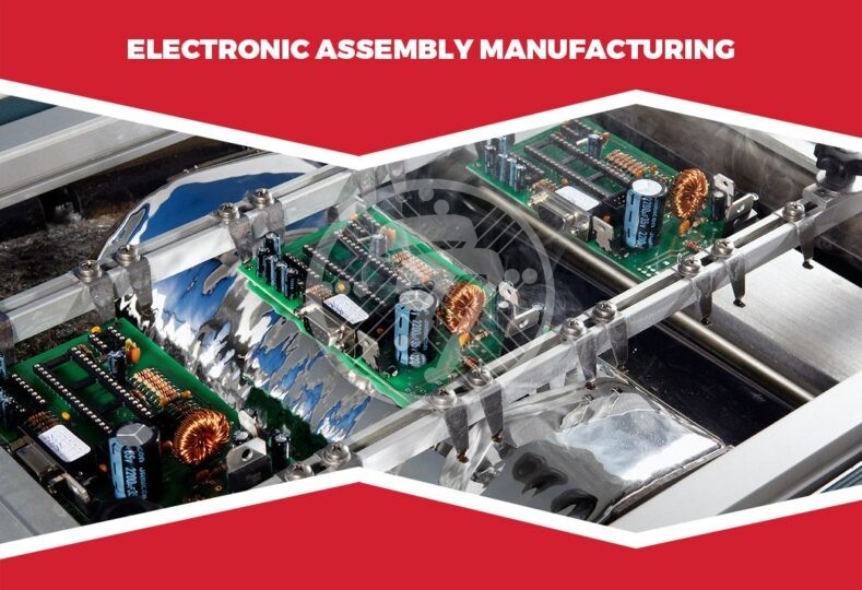
Best Long-Term Practices for Electronic Assembly Manufacturing with the Wave Soldering!

In this rapidly growing electronic industry, innovative ideas are very important to be in the market. Wave Soldering is an important feature for the electronic assembly manufacturing to run the PCB in the long term.
Nowadays, Wave Soldering reduces to a noticeable level, but its importance is still unreplaceable in long scale PCB Assembly.
As wave soldering is an important component of PCB, in this article, we broadly discussed it so that you can grasp a good idea about its importance.
What is the wave soldering process?
Wave Soldering is the process of providing the PCB electrical second soldering through a joint to make the PCB assembly more reliable, efficient, and long-term.
The wave soldering is done by both through hole mount or surface mount processes. But the surface mount process is most commonly used in the advanced infra-red wave soldering methods.
Factor Consideration of Solder Bridging in Wave Soldering procedure:
Myriad factors have to be analyzed at the process of solder bridging in wave soldering. From the component to the design process, everything has to impose only after a thorough investigation. The factor which has to evaluate are –
Length of lead:
The lead length used in the soldering has to be medium in size, if it becomes short, it will be unable to reach the capacitor, or if it is long, it causes webbing between the pins. A perfect lead length is that which can easily transfer the heat. The best way to measure the almost exact size is by the ratio of design and PCB’s thickness.
PCB Designing Consideration:
Pin count is a factor to consider at the time of design of wave soldering in electronic assembly. For the significance bridging two or more than two-row parallel pins are the perfect number.
For fine pitch, must confirm that a large number of perpendicularly oriented pins are present that influence the connectors of the bridging to do the work efficiently.
PCB Component Consideration:
Ensure that the axial and radial component of soldering is appropriately set up. This alignment of the components helps avoid most lifting crises.
An inappropriate positioning can cause increased length and can lift the element out of place.
Tooling consideration:
An appropriate PCB orientation is very important in tooling the wave soldering. In case of good waving, the board’s angle has to be between 15-30 degrees. That helps the pin to migrate when required. And it is very useful for large pins also where the connector is almost parallel to wave soldering.
The space between wave openings and the flow channel of the pallet of soldering is very important.
The height of the side of the button of the components of the surface mount process is also an important tooling consideration. It impacts the number of pallet requirements, the capacity of the flow of soldering. The length versus width ratio is a key component of any defect in it hampered the flow of soldering and another wave deformity.
Process Consideration:
In the process, the wave length, the flow ratios between lands and lamina waves are examined. With the rise in the ratio, the component of the PCB lifted. The height of the wave is less than half of the PCB thickness to reduce the chance of turbulence flow. Not only the height ratio, other factors like the angle of the pallet, but the oscillation of the conveyor also has to be considered.
Design consideration:
For the best design of the wave soldering the copper, the layer is directly connected through a hole to the wave plate. It works for the proper flow of heat, which is good for adequate thermal relief.
The second thing to consider in design is the ratio of lead diameters with the through-hole diameter of the PCB plate. The ratio measuring 0.6 is the best for wave soldering.
Solder Void:
Soldier void is very important because any problems in it cause moisture problems in the PCB. The voids are small holes that entrap gas during soldering, which outgasses the joints because most of the PCB is moisture sensitive, and this out grass process makes the cabinet dry.
Solder Ball:
A solder ball is aimed to adhere to the wave soldering process at the point it requires. Solder ball controls the flux application. It resists the flux when its flow is high, promoting the wave when the flux is low. Thus, it controls the temperature of the Assembly also.
Conclusion:
The Wave Soldering is recommended to the manufacturer who wants to handle a long-term Electronic Assembly. Most manufacturers don’t consider it, so it will be a good point to make a difference. With the market’s evolution, you also have to be evolved to challenge the industry and fulfil users’ demands.
Technotronix is a leading PCB Assembly company which has been operating for the last four decades. We are upgrading ourselves every day and offering the finest circuit board assembly, circuit board designs and fabrication services to our clients. We overcome every challenge that our customers can face, which helps to get perfect momentum in PCB making. The PCB designing results from Technotronix to evolve with time and easily place their place in the global PCB market.
Get a Free quote for PCB Assembly!


