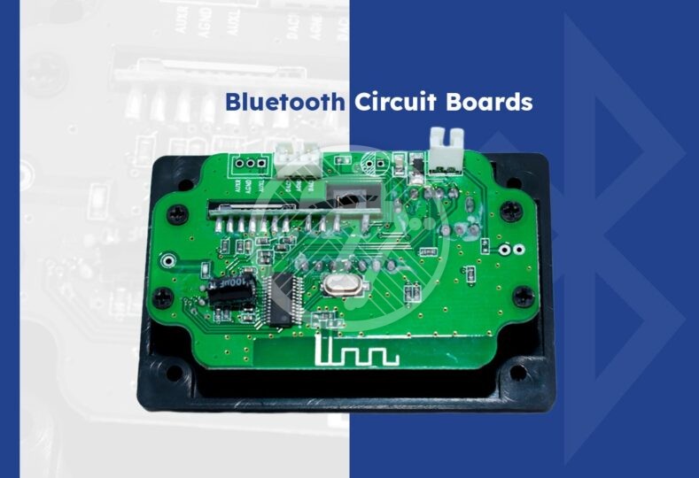
The best design guidelines for Bluetooth Circuit Boards!

The use of devices that utilize Bluetooth is becoming quite ubiquitous. From headsets and audio products to home automation systems, wireless consumer electronics applications, the list is ever growing. When it comes to designing PCBs with Bluetooth technology there are a number of issues that you can contend with, including but not limited to:
- Signal Integrity
- Interference
- Lost data, and more.
It is, therefore, imperative that certain design guidelines be followed to optimize signal integrity and ensure overall device effectiveness. Before we look at some design guidelines in detail, let us first look at the components of a Bluetooth Circuit Board.
Components of a Bluetooth Circuit Board
The vital components of a Bluetooth Circuit Board include:
- An antenna that helps in sending & receiving information.
- There are also inductors that adjust the impedance of the antenna.
- Module containing up to 4 IO pins.
- Diodes, resistors & capacitors.
- Chips and regulators.
On account of a number of sensitive components it is important that they be handled extremely carefully.
Let us look at some design guidelines that need to be followed when it comes to Bluetooth Circuit Boards.
Bluetooth Circuit Boards design guidelines:
Certified Modules
While incorporating Bluetooth, it is prudent to use a pre-certified module. With its use, development can be accelerated & time-to-market significantly enhanced. The availability of certified modules that include an ARM processor offers flexibility and power.
Bluetooth Device Selection
It is important to choose an appropriate Bluetooth device & to ensure that the antenna is sized. For simple beacon applications, Bluetooth Low Energy can be used, however for higher throughput, you need something with more Tx power and faster data rate. However, you could also use an all-in-one chip with powerful processors.
Power consumption
It is important to calculate the power consumption and to ensure that there is no current leakage in the design. The use of a microcontroller can ensure longevity of your device.
Separate Copper Signals
Keep the antenna area free from any copper signals nearby as also from high-energy components. It is also important to keep the area free from planes & polygon pours. If the antenna area is being manually laid out, it is important to use a ground plane.
Also, it is important to use ground stitching vias. By doing this you will ensure that unwanted radiation from the PCB edge does not penetrate the Bluetooth signals.
Another best practice to follow includes optimizing the board shape as per the Bluetooth device. It is also important to separate the analog & digital ground planes.
Power Supply Notes
It is important to ensure that the rail that supplies power to the Bluetooth module is kept clean. Also the use of bypass and decoupling capacitors is recommended. In order to reject high frequency noise the use of ferrite beads on the power rail is recommended.
Tools and Analysis
In designing the antenna area, it is important to analyze as well as tune the matching network. For this you need to have proper network analyzers.
Take care of Real-World Obstructions
There can be a number of real world obstructions to a Bluetooth connection. These could be by way of smart phones, computers, microwave ovens, office lightning and more. All of this can cause signal loss. In order to make sure than signal quality is not impacted a higher power device is recommended.
EMI Shielding Strategies
The use of EMI shielding strategies such as increasing the distance between traces or by adding an EMI shield can ensure that high frequency coupling does not reach the components.
Physical size constraints
A wide variety of Bluetooth PCB devices are portable and therefore needs to fit into an enclosure. The design therefore needs to take into account these constraints. What is also important is that you look at the board real estate management since your device would be performing other functions. This could necessitate the use of WiFi cards, analog microchips and more. All of these components will compete for space and hence the choice of proper sizes is important.
To Sum Up
By following the above guidelines at the design stage you can make sure that you avoid issues at a later date. Partnering with an experienced PCB manufacturing partner can go a long way in ensuring success of your Bluetooth Circuit Boards. Without due emphasis being laid to the design aspect the overall device performance can be severely affected.
At Technotronix, we are fully equipped to handle your PCB manufacturing requirements. We follow industry best practices to ensure we deliver cutting-edge products. If you have any questions or any requirements related to printed circuit boards, please feel free to contact us via email at [email protected] or call 714/630-9200.


