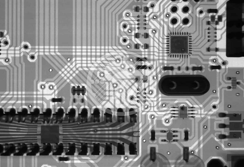
Why choose Automated X-Ray Inspection (AXI) Technology in PCB Assembly?

Simply put, Automated X-ray inspection or AXI technology as it is popularly referred to, uses X-rays to inspect the features of target objects. As an application, it finds place in a whole lot of industries today including but not limited to aerospace, medical, PCB Assembly and more.
X-rays go a long way in testing PCB quality as traditional inspection devices have their own limitations especially when miniaturization is on the increase. Also there are added issues of solder joints being hidden in some cases. X-rays however can penetrate and inspect quality of hidden solder joints as well. Therefore, while Automated Optical Inspection is only applicable for defects that are relatively easy to spot, such as open circuits or solder bridges, Automated X-ray inspection is required where inspection isn’t possible basis light alone.
The advantage with X-rays comes on account of the fact that materials absorb X-rays proportional to their atomic weight and depending on their density and thickness. Heavier elements thus absorb more X-rays as compared to lighter ones. Hidden defects, therefore, such as those to do with missing electrical components, shorts etc are far easy to catch.
An ideal X-ray system however must have clear images so that information with respect to defect analysis is clear and actionable. It is ideal, therefore, that the X-ray inspection system has adequate magnification as well as oblique angle inspection function. The latter ensures that solder balls aren’t just inspected from above.
X-ray inspection devices typically come in two forms- two- dimensional and three-dimensional systems. Both these can be operated off line and therefore make the inspection process easy. Some devices however can be used online. The choice of offline versus online devices typically depends on the amount of inspection required. In cases where there are large quantities to inspect and the level of inspection is complex, online devices are generally used. While a two-dimensional system can display 2D images of components from both sides, a three-dimensional system can generate images of cross sections. 3D systems can also combine images of a cross section in a method known as laminography.
The kind of resolution required also necessitates the need to choose the right X-ray tube, which is typically available in two categories- open and closed. Also the amount of magnification required determines the distance between the sample and X-ray tube. The X-ray voltage is yet another determinant of its penetration capacity. With a large voltage, objects with high density and thickness can be inspected easily. With single sided boards, however it is enough to go with low voltage. Similarly multi-layered boards call for high voltage.
The early inspection devices came with an image intensifier linked to a CCD Camera, the image intensifier, however, came with the following constraints:
- Limited range- The limited range in turn implies that the area may need to be inspected with more than one technique. This in turn increases the time taken to satisfactorily carry out the inspection.
- Limited field of view- At a given point in time a three to five inch diameter areas can be inspected.
- Image blooming- There is a chance of the image bleeding at the edges as the ionizing radiation passing by the edge of the casting is not attenuated
- Increased Noise levels- The image intensifier produces a noisy image. A clean, noise free image necessitates a digital processing of the image, which in turn is time consuming and does not let the process remain real time.
The above constraints however can be mitigated with the use of a direct digital imaging device. It not only offers a larger inspection area but also an improvement in resolution.
WITH X-RAY INSPECTION, WE CAN DO THE FOLLOWING:
- Perform a non-destructive inspection
- Locate short circuits
- Detect voids in solder joints
- Determine displacements of components
- Examine semiconductors
- Check switches, relays , plug and cable connections
The advantages of Automated X-ray inspection technology are as below:
- Reliable and consistent results
- Reduced time for inspection
- Reduction in labour cost.
- Effective process control as defects can be found in the early stage of the PCB assembly process and that it stops defects from flooding among the remaining PCB assembly.
Overall, therefore, X-Ray inspection technology is certainly a boon for PCBA manufacturers as it helps them improve product quality significantly. With the need for sub-micron resolution and extremely high definition images at high speed, the need for and the complexity of X-ray inspection technology will only grow. The way forward will be to be able to reduce the number of expensive operators as also remove the probability of human errors, if any, in the inspection process. This can be achieved by developing some inspection algorithms to be able to tackle these complexities.
At Technotronix, we are fully equipped to handle your PCB manufacturing requirements. With over 4 decades of experience in PCB manufacturing as well as PCB assembly with differing levels of complexities, we follow industry best practices to ensure we deliver cutting-edge products. Our team of experts and state-of-the-art equipment ensures that all our PCBs meet the industry standards of quality and testing. It is our vast portfolio of satisfied clients that stand as the biggest testimony to our success. In case if you have any questions, please feel free to contact us via email at [email protected]


