All about circuit board schematics that you should know!

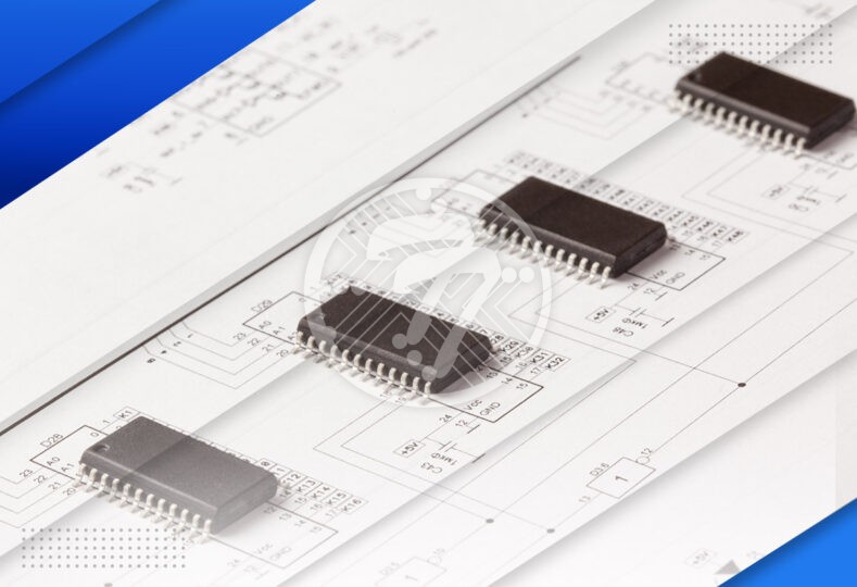
If putting together a functional circuit board was likened to putting together a tasty dish, the circuit board schematics would have to be the recipe that makes all the difference.
What really are circuit board schematics and how do they work?
With the increasing trend towards miniaturization, an electronic circuit board can be quite complex. Essentially a schematic diagram gives you information about which components are used & importantly how they are connected to each other.
With a dense topology, PCB diagrams become increasingly important. In fact the importance of a PCB diagram can be adjudged if one was to look at the sheer number of processes that are involved in making a circuit board.
The PCB fabrication process itself consists of sub processes such as imaging, etching of layers, arranging the layers, drilling holes, plating vias, applying solder mask, silk screen and more. This is followed by the printed circuit board assembly process, which comprises of picking & placing components, soldering, cleaning, and more.
A circuit board schematic makes the circuit easier to understand and helps tremendously in board development and production.
Difference between PCB Schematics & PCB Design
Often times the terms PCB schematics as well as PCB Design are used interchangeably. The fact remains that they aren’t the same. While a PCB schematic is a two-dimensional circuit design that shows connectivity between PCB components, a PCB design, is a three dimensional layout. The PCB schematic plays an important role in the PCB design. While a schematic lays down how the PCB will finally achieve the desired connectivity, the design becomes the physical representation of the schematic and shows location of components as well as their connections. It is the PCB design that allows engineers to build the PCB.
Building Blocks for a Circuit Board Schematics
Here are some of the building blocks of a schematic:
Cover Page – As its name suggests, it gives an idea of the contents of the schematic. Simply put, it enables you to understand the scope of the product.
Project Statement -This delineates the purpose of the project, its goals & targets. Essentially it offers a high level understanding of the project which makes understanding the rest of the schematic, simpler.
System Block Diagram – This explains the features, functions & the modules that are required to make the product.
Component Schematics of every block – These are circuit diagrams of each functional block. On this basis the costs of the components and the board prices can be determined.
Standard Consistent Reference Designators – The Alpha-Numeric reference designators give an idea of the devices placed. These help us interpret the schematic easily.
Mechanical Components – Essentially these offer details of the devices that may not be a part of the board but which are needed for the final product.
Parts Library – Ensuring that the parts information is critical so that there is minimum rework at a later time. This will also ensure that creation of the BOM is smooth.
Revision Notes – A good set of notes will ensure that there is no confusion in the case of revisions.
Title Block – A title block with the name of the project, the designer, date it was created comes in handy in quick identification.
Below are some important aspects to follow when it comes to the circuitry, to ensure that the circuit board is readable & usable for different stakeholders.
Logic Flow
It is important that logic & connectivity is consistent especially when it comes to high-speed circuitry. It is the basis of the logic flow of the schematic that signal paths will be put together.
Legibility
While this may seem obvious, the fact remains that in a dense schematic with a lot of symbols, nets & pin numbers, you need to ensure that everything is legible. In its absence there can be guesswork, which comes at its own price. It is important to ensure that the reference designators, part numbers & more are not covered.
Creating Net & Component Classes
Creating different net & component classes will ensure that you take into account the design constraints specific to these classes.
Properties
The use of a property editor can ensure that you can adjust the properties in the schematic, such as the values of a selected part & more.
Text Information
It is imperative that the schematic contains text information such as:
- Part Numbers
- Product information
- Company contact, and more
Design Rule Checks
The importance of this aspect cannot be over emphasized. It is absolutely imperative to run a Design Rule Check in a schematic. This will ensure that there aren’t costly errors to contend with at a later date.
Simulation and PCB Layout
While following the points above, you will ensure that you make sure that your circuit board doesn’t have any connectivity errors, but you still need to make sure that the circuits perform well. You can make sure that this happens by running the schematic through a simulator. Any unexpected behavioral issues will show up in this process. Needless to say, that it ensures that you do not have to spend time & money designing several breadboards.
A final design check & you are ready to transfer the circuit board schematic into the PCB layout.
Technotronix provides a one-stop solution for PCB manufacturing services. With over four decades of experience in delivering high-quality, on-time, competitive price products, you can bank on us for your PCB requirements. In case if you have any questions, please feel free to contact us via email at [email protected] or call us at 714/630-9200.


