How Boundary-Scan Testing is Beneficial for PCB Assembly?


When it comes to PCB assembly testing, it is quite common to look at it like an added expenditure as opposed to viewing it as an essential quality control measure that makes a significant value addition to the final product. Even before looking at how boundary-scan is beneficial for PCB Assembly testing, it is important to answer the question of why one needs to undertake PCB Assembly testing in the first place.
The answer to why test, simply lies in the fact that it is the only way to ensure a quality product. Instead of looking at it as an expense, therefore, it needs to be looked at as a mechanism that saves the company costly mistakes at a later date, which in turn, can cost time, money and importantly company reputation. Inadequate testing can on the other hand lead to faulty products reaching the end consumer which may need replacement, may need to be recalled, can lead to irreversible dents to company reputation and even lead to costly lawsuits.
What is imperative is that the right amount of PCB Functional testing is ascertained so that you are sure of the quality of the product, without the testing costs, skyrocketing. The amount of testing can of course, vary across industries. Mission-critical operations, for example, will require extensive testing while there could be some industries where a certain amount of product defects could be acceptable.
Main elements of PCB Assembly testing

There are three aspects that need thorough evaluation, when we speak of the testing process. These include:
- Structural devices
- Structural connections
- Functional connections
To test all these three aspects, a number of testing methodologies can be utilized:
- Visual Testing
- Automating optical inspection
- X-Ray inspection
- In-circuit testing
- JTAG boundary-scan
- Customized testing software
It is imperative that the testing methodology employed, can cover a whole spectrum of potential fault categories so that a defect coverage score can be ascertained. This largely involves an approach popularly called PCOLA/SOQ/FAM. Essentially this is an end-to-end approach that covers the entire spectrum of testing as below:
PCOLA
This part deals with the structural devices and relies on visual testing. An acronym for Presence, Correctness, Orientation, Live and Alignment, it studies all these aspects carefully to ensure there are no defects found.
SOQ
Unlike PCOLA, which relies on visual testing, this part relies on electrical testing methods. SOQ is an acronym for Shorts, Opens and Quality and undertakes connectivity tests so that there is no issue with the electrical connection.
FAM
This aspect refers to functional testing and checks for Features, At-speed and Measurement. These tests are therefore able to ensure that the system functions as per set benchmarks.
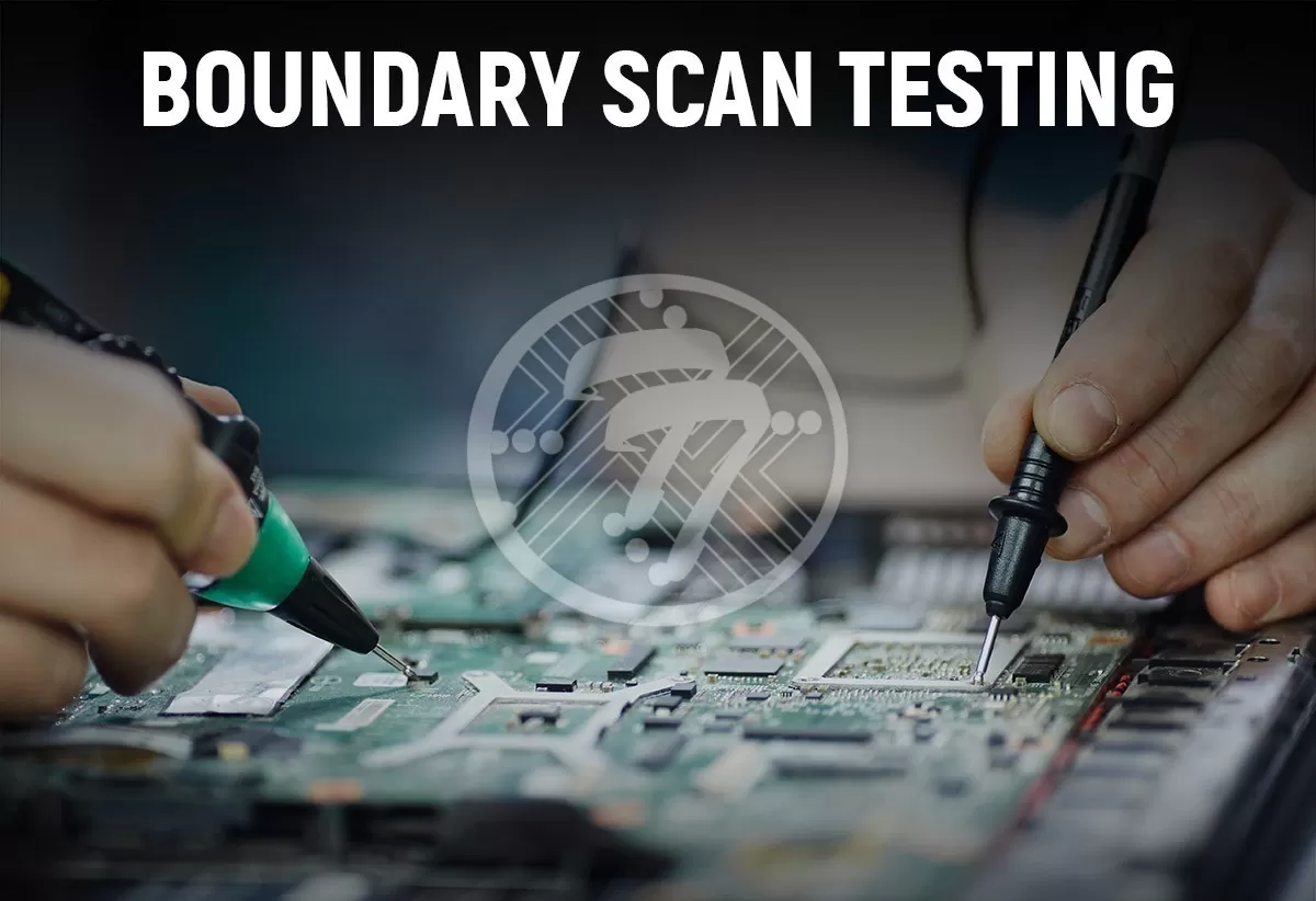
The relevance of Boundary-Scan for PCB Assembly
In the interest of cost, it is imperative to figure out which testing methodologies need to be used, which cover this entire spectrum. This is where boundary-scan becomes extremely relevant. The big advantages with boundary scan are as below:
- It is extremely relevant when physical access is limited
- It covers a significant portion of the PCOLA/SOQ/FAM spectrum and therefore offers breadth of coverage
- On account of its vast coverage, it takes away the need for other structural testing methods and thereby saves cost.
- It is far less cost intensive than methods like ICT, for example, which among other things require test fixture and equipment maintenance. While JTAG boundary-scan does need costs such as equipment, training, labour expenses etc. it still works out to be far more optimal as far as overall cost is concerned.
- It offers low test time, which in today’s day of intense competition is a huge advantage as it leads to quicker time-to-market.
- Needless to mention that it comes with product yield increase, which is the very purpose of testing.
In choosing the testing method, it is imperative that various aspects are taken into consideration. These include the coverage provided, the cost incurred and more. It is on all of these parameters that boundary-scan stands out. It offers both versatility and affordability. Little surprise then that it is one of the most popular methods when it comes to PCB Assembly testing.
Technotronix is one of the leading printed circuit board manufacturers based in the USA. We have over 4 decades of experience in providing innovative PCB manufacturing services using modern technologies and latest machinery. We are adhering to strict high-quality standards and compliant with the RoHS quality management system. To know more, please explore our PCB assembly services!