Standard 4-Layer PCB Stack-up: Design, Fabrication, and the cost of manufacturing!

By | Date posted: | Last updated: February 2, 2023
4-layer pcb stackup

With miniaturized electronic products becoming ubiquitous, the need for small circuit boards is on the rise. Multilayer circuit boards are therefore the order of the day. A 4-layer PCB stackup is becoming increasingly common. Let us look at the 4-Layered PCB in detail.

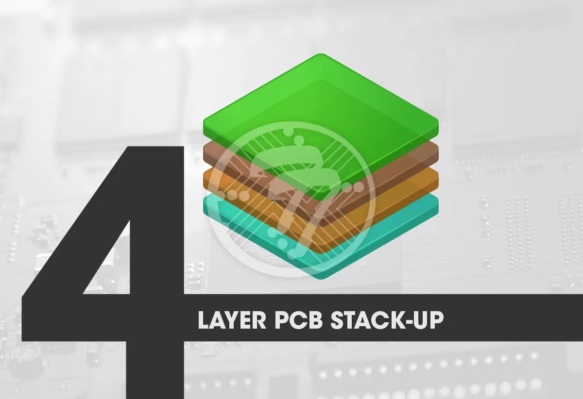
What is 4-layer PCB Stackup?

As its name suggests, a 4-layered PCB comes with 4 layers, these include a top layer, a bottom layer & 2 inner layers.

Of these 4 layers, 2 are signal layers, one VCC & the other GND.

Typically, the inner layers are used as power & GND, while the outer layers are used for routing of signals as well as for component placement. With the inner layers used as power and GND planes you can be sure that EMI emissions will be less, and the quality of signal will be robust.

4 Layer PCB Advantages

The 4-layered PCB offers several advantages, including but not limited to:

  • Improved routing of signals
  • Better EMI shielding
  • Improved thermal control
  • High assembly density
  • Lends itself to compact designs and to miniaturization

YOU MAY ALSO LIKE: Single Layer VS Multilayer PCB

Structure of standard 4-Layer PCB design stack up

There can be 3 ways in which these can be stacked up

Option 1

  • Top Layer – Signal Layer
  • Inner Layer 1- Power Layer
  • Inner Layer 2 – Ground Layer
  • Bottom Layer – Signal Layer

It is important to note that the less the distance between the power and the ground layer, the less will be the impedance.

Option 2

  • Top Layer – Power Layer
  • Inner Layer 1- Signal Layer
  • Inner Layer 2 – Signal Layer
  • Bottom Layer – Ground Layer

In this option, the power and the ground layer acts as a shield for the inner signal layers. However, on account of the distance between the power and ground layer, the plane impedance tends to increase.

Option 3

  • Top Layer – Signal Layer
  • Inner Layer 1- Ground Layer
  • Inner Layer 2 – Power Layer
  • Bottom Layer – Signal Layer

While this stack-up is like the first one, here the key signal layer is the top layer.

4-Layer PCB Stackup Thickness (Core and Prepreg Thickness)

4-Layer PCBs come with two types of Core & Prepreg thickness. The standard thickness is 1.6 mm (about 0.06 in) although 1.2 mm (about 0.05 in) is also commonly used.

We have already published article where you can check difference between PCB core and prepreg .

With a 1.6 mm (about 0.06 in) PCB, the core material is 1.2 mm (about 0.05 in) thick while the prepregs are 0.2 mm (about 0.01 in) each.

With 1.2 mm (about 0.05 in) thickness, there is a core material of 0.8mm (about 0.03 in), o.2 mm (about 0.01 in) of prepreg with coil and 0.2 mm (about 0.01 in) of prepreg with copper.

4 Layer PCB Manufacturing Process

Broadly the steps involved in manufacturing are as below:

  • #1. Clean up using the chemical method
  • #2. Lamination of the dry film
  • #3. Exposing and developing the image of the Inner Layers
  • #4. Copper Etching
  • #5. Strip Resist
  • #6. Layer up as well as bond with prepreg
  • #7. Layer up with Copper Foil
  • #8. Drilling
  • #9. Plating & deposition of copper
  • #10. Imaging of Outer Layer
  • #11. Copper Plating
  • #12. Tin Plating
  • #13. Etching
  • #14. Application of Solder Mask
  • #15. Applying the appropriate Surface Finish
  • #16. Application of Sun Screen
  • #17. Electrical Testing
  • #18. Profiling as well as V-Scoring

4 Layer PCB Cost

When it comes to the cost of a 4-layer PCB, there is not a standard cost as it depends on several factors. Some of these factors include:

  • The size of the board.
  • Material used. Here there can be variations from a standard FR-4 board to a high Tg material, which is more expensive.
  • Complexity involved in manufacturing. Typically, when the PCB has buried and blind holes, the complexity increases and so does the cost.
  • Thickness of copper.
  • Choice of Surface Finish. Typically, if finishes like Immersion Gold are chosen, the cost will increase.

YOU MAY ALSO LIKE: Ways to reduce PCB assembly cost

Sum up

It is important to make the right choice of PCB contract manufacturer who will be able to understand your bespoke requirements and fabricate your board according to your needs.

Technotronix is equipped with industry best practices. As a professional manufacturer with 40 years of experience who ensure that you do not have to reinvent the wheel. Technotronix provides PCB assembly and PCB fabrication service. Besides that, the cost and the turnaround time are also optimized so you will get a competitive advantage.

Top factors that can drive up PCB fabrication cost!

By | Date posted: | Last updated: March 18, 2026
PCB fabrication cost

When it comes to PCB fab, there are a wide variety of factors that affect its PCB fabrication cost. Right from the size of the printed circuit board to its layer count, these factors have a strong bearing on the cost that you will incur in fabrication. A detailed understanding of these factors will help you fabricate a printed circuit board that meets your requirements as well as your budgetary constraints.

Factors that impact PCB fabrication cost

1. Size of the PCB

Both the size as well as the shape of the PCB strongly influences its cost. Typically, the cost of the PCB increases with the increase in its surface area.

Commonly used dimensions include:

  • 18 X 24″ (457 x 610mm)
  • 18 X 21″ (457 x 533mm)
  • 21 X 24″ (533 x 610mm)

Additionally, the price is also affected by the space that is consumed by the components on the PCB.

2. Layer Count

As more layers are added to the PCB, its cost tends to go up. This stands to reason as additional layers means more material as also increased fabrication time. Additionally, it is important to remember that with a high number of layers the odds of developing defects also go up. The testing costs for high layer PCB therefore are also high. As a thumb rule, adding 4-6 layers increases the cost by around 30-40%.

YOU MAY ALSO LIKE: Multi-Layer PCB fabrication process

3. Complexity

The more complex your designs and configurations, the higher your cost. This is because complex boards come with additional processing steps, which involve the use of machines or manual labor.

4. Choice of Material

It is important that you choose PCB material that meets your requirements and fits your budget. This is because high-quality material for specialized board functions comes at an added cost. The choice of material, in turn, is influenced by several factors including but not limited to:

  • Thermal reliability
  • Heat Transfer
  • Signal Performance
  • Mechanical Properties, and more.

5. Trace and Space

Should you opt for tight traces, they come with challenges in etching and hence impact the price. On the other hand, enlarging the PCB trace width or adding solder mask to the traces also adds to the price of the PCB.

6. Hole Size

If the requirement is for small hole sizes, it stands to reason that it will require special tools or lasers for precision. In turn, this will impact the cost. Similarly, if the requirement is for a large number of holes, the cost tends to go up.

YOU MAY ALSO LIKE: How precise drilling reduce PCB fabrication cost

7. Controlled Impedance

With controlled impedance, it is imperative that there be uniform trace width. In turn, there are several requirements, be it of a certain kind of material or specialized testing procedures, all of which impact the cost.

8. Tight Tolerances

Once again tight tolerances in the PCB design add to the complexity of the board and lead to testing and troubleshooting costs.

9. Copper Foil Weights

If thicker copper is to be used, there is a direct correlation with the cost. Additionally, there is also the requirement to use added pre-preg, all of which have cost implications.

10. Solder mask/ Silkscreen

The use of solder mask/silkscreen adds to the time taken in fabrication, not to mention the fact that it requires distinct processes that may require distinct tools.

11. Surface Finishes

The choice of surface finish has a strong implication on costs. There are standard finishes like OSP that are extremely cost-effective. However, finishes such as ENIG, for example, can significantly add to the cost.

12. Custom Specifications

Custom specifications can go a long way in increasing the cost of PCB. Some of the custom specifications include:

  • Contoured edges
  • Solder Mask Clearance
  • Side-plating, and more.

If there are details in your design that aren’t commonly assembled, it could lead to added time in production, not to mention the fact that it could need specialized tools. It is thus important to calculate the potential cost of your design in advance, for you to undertake a cost-benefit analysis.

To sum up

To keep costs at a reasonable level, it is important to look at several of the above-mentioned factors beforehand. This will ensure that you keep the costs in check.

Go with a Technotronix – a professional PCB fabricator with 4 decades of experience and ISO 9001:2015 certified who is equipped with the necessary industry best practices. So, you do not need to undertake unnecessary trial & error beyond a point. You can fill out the PCB fabrication quote form or mail us at [email protected]

What should be included in a PCB fabrication drawing?

By | Date posted: | Last updated: December 11, 2025
PCB Fabrication Drawing

A PCB fabrication drawing is an extremely important file that contains the manufacturing details of the circuit board. The more diligently the PCB fabrication drawing is created, the better the chances of the circuit board matching your exact requirements. A fabrication drawing lays down the specifics of the circuit board such as the board outline, layer stack-up, drill chart and more. A fabrication drawing along with an assembly drawing together, comes in extremely handy in assembling the circuit board.

How does a PCB Fabrication Drawing differ from Assembly Drawing?

As their names suggest, a fabrication drawing provides essential details that are required for the manufacturing of the board. An assembly drawing on the other hand lays down details about how every component will be attached to the board.

What should a PCB Fabrication Drawing Include?

Some of the aspects that a PCB Fabrication drawing must include:

Dimensions

It is important to mention the dimensions of the board as that will determine how much PCB material is required. Typically, the areas that need to be mentioned include:

  • Length of the board
  • Its width
  • Thickness
  • Outline
  • Tolerances

There also needs to be a Board Outline, which includes the cut-outs, holes, radii, specific distances from the origin, and more

Drill Chart

There needs to be a detailed drill chart that offers the following information:

  • Which layers need drilling
  • Drill Sizes
  • Tolerance, and more.

The drill chart has specific symbols to do with the hole size. It offers information on whether the holes are plated or not and more.

Layer Stack Up

The layer stack up has a lot of influence on some of the other aspects of the project. It is therefore imperative to convey information such as:

  • Material
  • Thickness
  • Copper Weight
  • Surface Finish
  • Tolerances
  • Controlled Impedance

Basis the Controlled Impedance requirement, the manufacturer can then look at aspects such as the dielectric constant, spacing, trace width and more.

Title Block

The Title block consists of information such as:

  • Customer Name
  • Part Numbers
  • Fabrication Number
  • Measurement Units, and more.

PCB Fabrication Notes

In addition, it will help to include PCB Fabrication Notes with the following information:

  • Requirements of Controlled Impedance
  • Manufacturing specifications
  • Raw material specifications
  • Plating details
  • Details of Solder Mask
  • Gold fingers, if present
  • Any specifications related to hole positions
  • Presence of via-in-pad, if any
  • Blind/Buried via, if any
  • Tolerances, both in terms of board tolerance & plating & etching tolerance

The PCB Fabrication drawing can be created in a wide variety of software, including but not limited to:

Eagle EDA
This is one of the commonly used software where the process is fairly simple. The basic steps involved here include generating the PCB Gerber File. Next you need to go to the Layout Editor. This will enable you to use the drill symbols on the board. With all the information about the number of layers & board material compiled, the files can be sent to the manufacturer.

KiCAD
The basic steps here include adding the Title Block. You need to add all the dimensions of the board in the outline. Next you can use the Graphics Tool to draw the stack up. Information such as board thickness, layer thickness, tolerances etc. can be mentioned. On the fabrication layer information such as number of layers, IPC class of the board, solder mask color, type of pads and more can be added.

Altium Designer
You need to use a blank drawing format and then add the details to it. Fab Notes & Drill charts can also be added. The files are automatically linked to the design database of the tool

To Sum up

The PCB fabrication drawings provide a lot of critical, additional information that is not available by way of Gerber Files. With all the above information mentioned, you can make sure that there are no communication gaps remaining & the board is manufactured to the exact details required. Needless to mention that other than providing detailed PCB fabrication drawings, the choice of experienced electronics contract manufacturer can go a long way in ensuring that you receive quality boards. An experienced manufacturer is equipped with industry best practices that ensure that you do not need to reinvent the wheel.

With advanced methods of PCB fabrication, we give you the finest PCB fabrication services. The PCB fab services from our experts will take it to the next level by accepting every type of latest technologies.

Request a quick PCB Fabrication quote!

The Complete Guide on Printed Circuit Board Stiffener for Rigid-Flex & Flex Circuits!

By | Date posted: | Last updated: December 11, 2025
pcb-stiffeners

A printed circuit board stiffener plays an important role when it comes to offering mechanical support to a PCB. They are particularly helpful for flexible circuit boards, that given their name, are flexible and in need of stiffness in certain places.

Stiffeners are particularly required when components are placed in a flex zone & the weight of these components stresses the flex material. They are also of use where a rigid printed circuit boards surface needs to be created to place SMT pad components. Also, connectors that need multiple insertions need stiffeners so that the stress of the pads is reduced. Let us look at the uses of stiffeners in some more detail.

What are the various uses of PCB stiffeners?

Simply put a stiffener is used where a certain area of the circuit needs to be hardened. Here are some of the common reasons for which a stiffener is used:

  • Supporting areas of the board that have SMT or PTH components.
  • Maintaining legitimate thickness of the flex circuit.
  • Supporting PCB connectors.
  • Ensuring better handling of the circuit board.
  • Ensuring that areas of the circuit board are kept stable.
  • Helping in routing and retaining arrays.
  • To help in strain relief as well as effective heat dissipation.

Broadly, flexible PCB stiffener requirements fall in the following usage categories:

  • Rigidizing Component / Connector areas
  • ZIF (Zero Insertion Force) Thickness Requirements
  • Localized Bend Constraint(s)

Component / Connector Stiffeners
Essentially, they create a rigid area where components and connectors are attached. They also protect solder joints by ensuring the flex doesn’t bend in the component area.

ZIF Stiffeners
They ensure that the thickness is increased at contact fingers to meet specific ZIF connector specifications.

Localized Bend Constraints
They restrict bend areas to specific locations in a flex design.

How to select the right PCB stiffener material?

Typically, PCB stiffeners are made up of FR4 or rigid polyimide. One of the oft-used polyimides in PCB stiffeners is Kapton.

The thickness of a typical stiffener ranges from 0.002″ to 0.059″. The thickness of the Kapton stiffeners range from 0.002” to 0.010” and the thickness of the rigid stiffeners range from 0.008” to 0.059”. Broadly, of course the thicker the PCB stiffener, the better support it offers. However, the requirement of each design is different.

Some use cases also necessitate the use of stainless steel or aluminum as PCB stiffeners. The disadvantage with using those, of course, is the prohibitive cost.

How to use printed circuit board stiffeners?

In case of plated through-hole components, the PCB stiffener is located on the same side of the flex as the components. With this, access to solder pads on the flex circuit is easier.

It is also possible to attach stiffeners to both sides of a part however, in such cases the PCB assembly needs to go through an array configuration review.

When an assembly array is required for flex circuit designs, it is recommended to use the FR4 stiffener throughout the array border. By doing this, you eliminate the need for any additional tooling plates. Besides, it allows the parts to run through the automated assembly much like a rigid circuit board.

When it comes to attachment of a stiffener to a circuit, heat and pressure is used. A pressure-sensitive adhesive can also be used to attach PCB stiffeners.

Two popular types of adhesives include:

  • Pressure Sensitive Adhesives
  • Thermally Bonded Adhesives

To make the right selection of adhesives, some of the factors that need to be taken into account include:

  • Thermal Exposure
  • Chemical resistance
  • Adhesive capacity when it comes to different materials.

PCB Stiffener Considerations

When using stiffeners, it is important to note that they should overlap bared coverlay by .030” to relieve stress. Also, when using multiple stiffeners, the same stiffener thickness should be maintained.

To sum up

The advantage of using a PCB stiffener when we need a rigid area in the circuit, in order to protect components or connectors, cannot be overstated. By doing so you can ensure that the circuit doesn’t bend and that the integrity of solder joints is protected. It is common to use FR4 as stiffener material for rigidizing specific areas of the circuit.

At Technotronix, we are fully equipped to handle your PCB manufacturing requirements. With over 4 decades of experience in rigid-flex PCBs with differing levels of complexities, our team of experts and state-of-the-art equipment ensure that all our PCBs meet the industry standards of quality and testing.

For more information, contact us via email at [email protected] or call us on 714/630-9200.