Enhance the Quality of PCB Fabrication with HDI PCB Technology!

By | Date posted: | Last updated: April 8, 2022
Quality PCB Fabrication

If there is one trend when it comes to electronic devices, it has to be that of miniaturization. The size of electronic devices is shrinking and their complexity is on the rise. What this, in turn, means is the increase in demand of small PCBs. There is, therefore, a corresponding increase in the technology that can facilitate these small sized PCBs.

This is the exact reason why High Density Interconnect or HDI, as it is popularly called, is becoming increasingly relevant in today’s times.

What exactly is HDI technology?

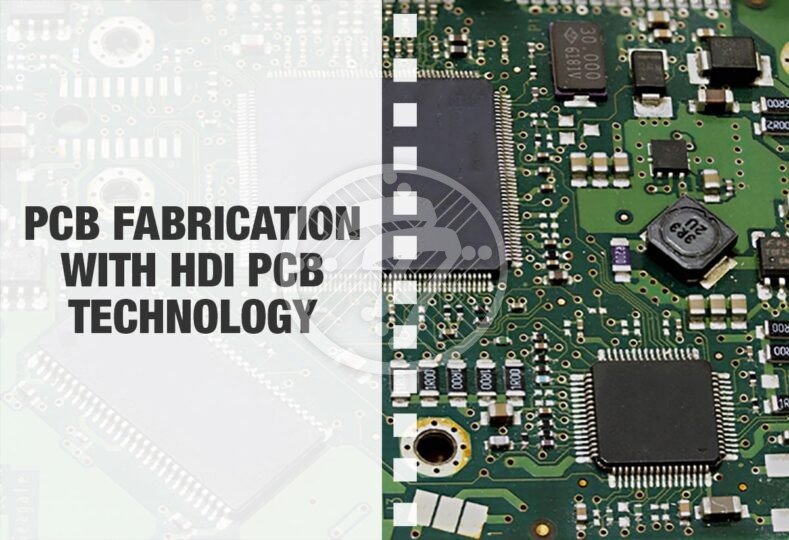
Essentially, HDI technology is a result of evolution in component packaging that facilitates the construction of small boards that can have a large number of components per square inch. Simply put, an HDI PCB, therefore, has higher wiring density per unit area, as opposed to a conventional board. HDI printed circuit boards with one or all of the following:

  • Microvias
  • Blind vias
  • Buried Vias
  • Other microvias
  • They also have built-up lamination and high signal performance.

In fact, it is the Microvias that have a huge role to play when it comes to the capabilities of HDI printed circuit boards. Since smaller vias can be close to each other, the board requirement is small. Also, space is easily freed up for additional components. With Microvias also having smaller aspect ratios that through-hole vias, the reliability quotient of HDI boards is far higher.

Importance of Using HDI PCB Fabrication

A typical PCB has one or two layers, while multilayer PCB can have up to 20 layers depending on their complexity. When it comes to HDI PCB, however, it could have as many as 40 layers which have densely mounted components, fine lines and micro vias. Some of the advantages of using HDI PCBs include:

  • The ability to have several permutations and combinations when it comes to the layers.
  • If you are looking for coreless designs, HDI PCBs come in handy
  • With via-in pad, what you can also have is the maximum number of components in minimal number of layers.
  • When it comes to mission-critical applications, The importance of HDI PCBs increase manifold.
  • They offer the highest level of accuracy
  • They have a better signal speed. The signal integrity is improved on account of shorter distance connections as well as lower power requirements.
  • Some of the other performance improvements of HDI PCBs include stable voltage rail, lower RFI/EMI, distributed capacitance.
  • It facilitates small cores and allows for fine drilling
  • It also facilitates microvias
  • It decreases power usage
  • It is extremely cost effective
  • It goes a long way in improving the overall performance of the device
  • On account of the design efficiencies that HDI PCBs offer, it also allows for faster time-to-market, which is a significant source of competitive advantage in today’s times.

Applications of HDI PCBs

HDI PCBs are used in a wide range of industries, especially where miniaturization is prevalent. These would include digital devices, automobiles, aircrafts and more.

Another area where HDI PCB Fab finds a lot of application is to do with medical devices. With the need for small devices with high transmission rates, HDI PCBs fit the bill. This is especially true of implants but also of other medical equipment such as CT scans, MRI equipment and more.

The TechnoTronix advantage for HDI PCB Fabrication

At TechnoTronix, we have over 40 years of experience when it comes to manufacturing high quality PCBs. Our superior technical expertise ensures that we design custom made HDI PCBs for your bespoke requirements at competitive prices. We cater to a wide range of industries including but not limited to:

  • Aerospace
  • Defense
  • Telecommunications
  • Medical PCB Prototype
  • Industrial PCB Prototype
  • Renewable Energy PCB Prototype
  • Rigid-Flex PCB Technology

If you are looking for best PCB fabrication services from product layout, manufacturing to warehousing and shipping, please explore our PCB fabrication services! We offer fast prototyping and consistent delivery of high quality products with quick turnaround times. We run extensive DFM tests to ensure that there are no costly errors later. The fact that we are an ISO 9001:2015 AS9100 Rev D company with unstinting focus on quality when it comes to PCB Fabrication ensures that you can rely on our services.

The Effect of Woven Glass Laminates on PCB

By | Date posted: | Last updated: April 20, 2021
PCB Fab

When it comes to increasing the structural strength of PCB materials, woven glass is an obvious choice. It adds significantly to the mechanical stability of the laminate rendering it high structural strength. In fact, the use of woven glass in PCB fabrication dates back as early as to the 1960s when they added high tensile strength and stability to the substrate. In addition, glass fibers also bring the added advantages of high thermal as well as chemical resistance, insensitivity to moisture as well as the advantage of being an electrical insulator. In the early days, however, there was little concern about considering the effect of inhomogeneity in the resultant substrate. However, today it is also important to understand how the properties of components affect the behavior of the whole.

Very often concerns regarding the negative impact of woven glass, in terms of electrical performance, come to the fore. The “glass weave effect” is feared to impact the performance of high-frequency PCB.

Here is an overview of factors that impact the woven glass weave phenomenon:

It is a possibility that on account of the woven glass laminate, the Dielectric Constant or Dk as it is popularly known as, varies across areas. So, in areas where glass bundles are present, the Dielectric Constant is high, while in open areas between the bundles, the Dk is low. The variation can be as high as between 6 in areas of glass bundles and 3 in open areas. Since Dk is an important metric, the variation in Dk is a cause for concern as far as circuit designers are concerned. Dk variation can impact performance particularly at higher frequencies of 30 GHz and above, also referred to as millimeter-wave frequencies. When the electromagnetic wave faces a change in the Dielectric Constant or Dk, propagation can be impacted and resonances may occur. The impact can be seen even when the anomaly is as small as one-eighth of a wavelength. With woven glass stacked to form a laminate, it is less likely for glass bundles and openings to align. Consequently, it is less likely for discrete Dk variations. In cases where two or more layers of glass are used, therefore, the impact of the glass weave effect is decreased.

The bigger issue regarding the glass weave effect, plays out when circuits use a laminate which has a single layer of woven glass. The fear also is to do with the random impact of the glass weave effect and how it will play out in case of high volume production. On account of the glass weave effect there can be performance variations from one circuit to another. Often changes in the phase angles of high frequency waves is noticed which in turn impacts phase based modulation.

This is not to say that using multiple layers of woven glass fabric can overcome all the issues related to the glass weave effect. Often differential conductors on a single layer circuit can bring about a new set of issues. In case the Dielectric constant or Dk values of the wave propagation medium varies between the pair of lines, the phase angles are impacted. This in turn, results in a slowing down of the propagation of one signal wave over the other and results in a skew. Particularly in high speed circuits, this can affect performance.

However, fortunately there are ways to tide over this issue. Changes in Dk can be stemmed by using a laminate with a filled resin system. The use of the filler results in less variation in Dk. The combination of glass fabric, resin and filler, in fact averages out the variation in Dk values thereby ensuring that performance is not impacted.

Yet another way to ensure that performance isn’t negatively impacted, is to use flat glass fabric along with minimizing the relative glass content in the laminate. This also goes a long way in minimizing the variation in Dk. The use of spread glass is also beneficial as it offers the ability to wet the fibers which allows a chemical bond to be formed between the glass reinforcement and the resin. This in turn, is a significant improvement over using traditional tightly bound bundles of glass fibers which can lead to defects in the interface.

The way to overcome the glass weave effect totally, of course is to not use woven glass at all. There are ceramic filled laminates that ensure that the dielectric constant or Dk is maintained in a certain range across the circuit board. This consistency, in turn, works well for small wavelengths as also for coupled lines.

In future PCB substrates will use even better fibers and resins to produce more advanced and functional materials that will add to the performance.

At Technotronix, we have over 4 decades of experience in PCB Fabrication. With our experienced PCB manufacturer, you can rest assured that what you will get is an effective production. Check out our PCB fabrication services. Also, you can drop an email to sales@technotronix.us or give us a call at 714/630-9200 to solve your queries or to get a quick quote!

Why Silkscreen Is An Important Method Of PCB Fabrication?

By | Date posted: | Last updated: February 14, 2022
pcb-fabrication-2

The term silkscreen has derived its name from the process of using a stencil on a PCB. Also referred to as legend, it refers to the text-based information that is printed on a circuit board. This includes information such as component references, company logos, component identifiers and more. It is commonly used on the component side to identify various components although sometimes it is used on the solder side as well. However using two silk screens tends to increase the cost. The standard colours are Black, white and yellow, although other colours can also be requested. Similarly silk screening can be done in a whole lot of fonts. However, the important thing to remember is the readability of the font.

Traditional silk-screening requires polyester screens stretched on aluminum frames. Besides this you need a laser photo plotter, a UV printer, spray developer and curing ovens.

Presently PCB silk screening can be done in either of three ways:

  • Manual screen-printing

    – This can be done when line widths are greater than 7 mil and its registration tolerance is 5 mil. While this allows for easy set up and application, it requires large texts and line width size. Also in terms of accuracy it isn’t the most desirable option as the output depends on a number of factors such as viscosity and age of ink, room temperature, amount of humidity, pressure of stroke and more.

  • Liquid Photo Imaging or LPI

    – This method is used when line widths are greater than 4mil. This is known to provide more accuracy than manual screening. However this has longer set up time and is known to use more ink.

  • Direct Legend Printing or DLP

    – This method is highest in terms of accuracy but also comes at a higher cost and also does not work on silver surface boards. Also not all fabricators have DLP Printers.

A well-designed silk screen plays a very important role as it can reduce both the likelihood of error as well as the time taken to spot the error. This is true both for the assembly process as well as during the rework phases. In fact, it isn’t sometimes necessary for the process to identify all the passive components that make up the devices on the board. Instead, it is enough if the silkscreen mentions the circuit functionality. In fact, for a PCB packed with many small components this is a far more achievable objective than labeling each and every individual component. While active components can be labeled, the passive ones need not be. Choosing to identify the circuit functionality instead of all the passive components, in turn, ensures that the silkscreen legend is useful as well as legible.

In fact a detailed understanding about silk screens can also go a long way in reducing PCB Costs. For example, silk-screening on one side only can reduce artwork costs. Similarly, restricting yourself to standard colours during the silk screening process can impact the cost of PCB fabrication, while keeping its benefits intact.

Technotronix is one of the kingpins in offering PCB layout and manufacturing solution to all predominant industries. With a strong team of technical professionals, it has gained expertise in providing PCB silkscreen to reduce PCB artwork cost used in PCB Fabrication. Our key success factor to achieve new heights in technological innovations is continuous improvement and high quality standards. You can drop an email to sales@technotronix.us or give us a call at 714/630-9200 to solve your queries or to get a quick quote!

The Fortunes Of Using Heavy Copper In PCB Fabrication

By | Date posted: | Last updated: February 15, 2023
pcb-fabrication

The PCB fabrication is now a kernel of technological trends in current times across the globe. With rigorous development in technologies, the electronic instrument and components are also showing a pace in innovation every other day as the global market trends have turned into a dynamic one with ever changing customer preferences and demand for unique electronic products. This is where the electronic manufacturer and PCB fabricator have the same concern for reliable, high quality, cost effective electronic solution even in case of complex critical pcb layout requirements. One of the recent growing trend in PCB fabrication is the utilization of heavy copper in PCB manufacturing. This article brings to light the enrichments of using heavy copper in printed circuit board fabrication. In addition to this, it also furnishes with the technical details on the construction of PCB’s with using of heavy copper substrate.

To suffice the increasing demand and preferences of customers from varied market, the trend of using heavy copper in PCB’s is becoming a “good show” to trap the present world of technology implementation. When we speak about printed circuit boards, they have their application in each and every aspect of human life. Right from telecommunication, medical, automotive, defense, aerospace, military to renewable energy, transportation, industrial sector and many other dominant industries. On the other hand, the demand for high tech electronic machinery and appliances that run faster, are compact, secured product to use and more efficient with high power performance is what the customers desire that keeps on moving ahead with introduction to new technology every other day. This has made the PCB industry to be on top of the heap when it comes to innovation and transformations. Be it a heat dispersion, fast speed, high frequency or other critical design requirements, heavy copper in PCB fabrication has proven high performance output. Check out the complete guide on Copper Balance in Printed circuit Board Fabrication.

When learning to cook a dish, we first tumble on the ingredients and recipe and then start cooking, the same way, lets get a clear picture on technical aspects of Heavy copper used in PCB manufacturing before taking a dive into understanding the core merits of the Heavy copper PCB.

The printed circuit boards manufactured with the use of heavy copper is constructed with a fine combination of copper plating and copper etching processes. As the thin sheets of copper foil, the layers are created with circuits. Further, the copper etching technique makes it possible to eliminate the unwanted copper and copper plating technology optimizes the copper thickness to Traces, Pads, Planes and Drilled holes on the circuit board. Final lamination of layers in circuit board is done using epoxy based substrate. These heavy copper PCB is made of thermo layers which is best suited in multilayer PCB construction. In short, the heavy copper PCB is fabricated with high usage of finished copper in the internal and external base of the circuit board that is also known as laminated deposition.

The fortunes of using heavy copper in PCB fabrication

  • Best for a compact electronic solution as it utilizes less space with either removing or allocating minimum space for cooling fans or heat sinks.
  • High current carrying capacity.
  • Resistance to high temperature.
  • High durable performance with use of heavy copper substrate.
  • Easy transfer of heat to external heat sinks.
  • High caliber to withstand repeated thermal cycling that is capable to destroy a normal PCB in flip of seconds.
  • Highly feasible to resist in rugged environments.
  • It has a high tolerance to thermal strains.
  • Attaining negligible undercut and straight side walls with a fine combination of plating technology and copper etching technique.
  • It is proved rough and tough with low impedance in power distribution.
  • The heavy copper in the circuit board also can develop a connection with standard circuits.
  • With the implementation of heavy copper plating technology, high current circuits are generated that helps to observe simple and dense beard structure.
  • High reliability of electronic performance by using heavy copper pcb layout or extreme copper PCB.
  • The heavy copper concept is now successful with even blending with the standard attributes on a single circuit board that is well known as PowerLink.
  • The use of heavy copper in PCB fabrication makes it possible to attain smaller footprints and reduced layer count on the circuit board.
  • Increased mechanical strength in plated through holes and at connector sites.
  • It is possible to use exotic materials in heavy copper pcb layout without circuit failure in case of high temperature conditions.

The other main reason of high usage of heavy copper PCB’s is the reduction of critically complex wired buss configurations. With these riches of heavy copper PCB’s, the researchers are now heading towards the efficient method to implement unique PCB Layout for complex requirement with making it more cost effective along with delivering high quality in PCB fabrication.

Technotronix is one of the kingpins in offering PCB layout and PCB manufacturing solution to all predominant industries. With a strong team of technical professionals, it has gained expertise in providing heavy copper PCB solution. Our key success factor to achieve new heights in technological innovations is continuous improvement and high-quality standards. Our team of experts and state-of-the-art equipment ensures that all our PCBs meet the industry standards of quality and testing. In case if you have any questions, please feel free to contact us via email at sales@technotronix.us