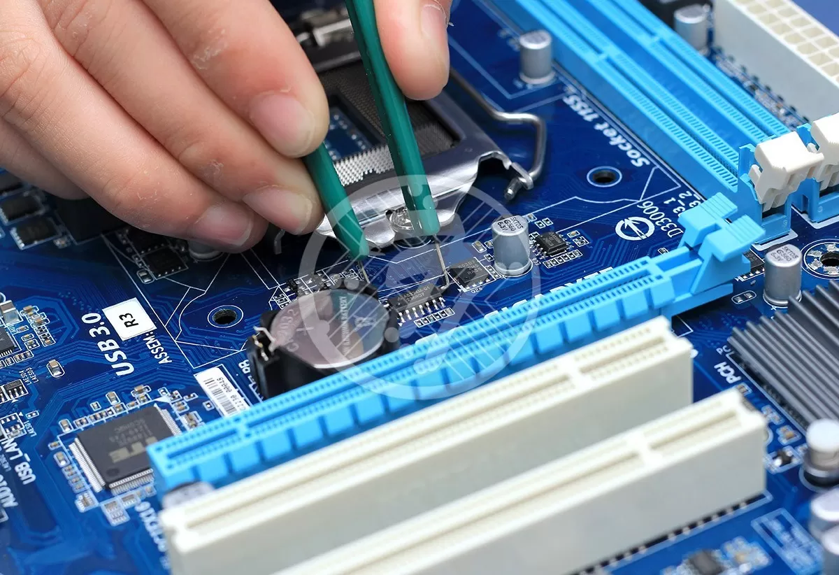
How Technology Is Rolling Up Its Sleeves for PCB Fabrication Approaches On RF and Microwave Performance?

By | Date posted: | Last updated: April 14, 2021
Microwave PCB

Changing the trend of the way we do business today with high application of right communication tool that is an exact fit for your business purpose has now become one of the success mantra for every business verticals. With new models launching every other day in smartphones, tablets, laptops and other communication gadgets, the printed circuit board industry have taken a step ahead to deliver optimum electronic and design solution to suffice the requirements of manufacturing process for modified communication tools making it pretty easy for manufacturers to come up with new technology innovations. With this, the microwave and radio frequency printed circuit boards have become preeminent part of manufacturing major electronic equipment. This article will lay down insights into the technicalities of microwave PCB or radio frequency printed circuit boards with considering new PCB fabrication approaches to get an exact electronic and design solution that can get the high pace of signal speed in electronic instruments.

The new era of modernization in communication equipment and tools used in the day to day business process has marked a high scope of expansion in development for all dominant industries. With the use of Radio frequency and Microwave PCB, the PCB experts and fabricators came up with a completely new range of innovation in the global market. The microwave PCB’s have become a niche domain of expertise to grab and locate the exact needs of the electronic manufacturers. Also the Radio frequency PCB is one of the tough electronic designs that has high stability when the amplitude, current levels and voltage vary as per the climate.

Lets first dig into details of RF and microwave PCB!

The term microwave circuit is derived from a Greek word ‘micros’ which means little or small. In the microwave or radio frequency circuits, the wavelength is small in comparison to the physical variation in an electric circuit and variation in the component size that accounts for high speed in signals. It has laminates that have mechanical, electrical and thermal characteristics that are not found in FR4 materials. This type of PCB was introduced in the market in the 20th century. With this, many new microwave circuit methods were an output of research and development which included microwave integrated circuit (MIC), waveguide and coaxial technology, monolithic microwave integrated circuit (MMIC) and many more.

The printed circuit boards that are used in avionics and wireless circuit applications that control operations on medium to high frequency modes majorly used in communication signals are known as radio frequency PCB or microwave PCB. The Radio frequency circuits has its application to specific feature rich pcb layout that is best installed right from military radars to laptops, cell phones and many more.

The difference between normal printed circuit board and microwave PCB:

The main difference between the two is physical and electrical properties of dielectric slab. Normally the radio frequency range is 500 MHz – 2 GHz. In case of layouts above 100 MHz are considered RF PCB and that above 2 GHz will be considered microwave frequency range.

How the signal speed works out well with high performance microwave PCB?

  • The important PCB fabrication approaches to make the devices have high performance output should be considered by PCB fabricators to provide best modifications with custom features in microwave PCB or RF printed circuit boards. Check out the top design guidelines for RF and Microwave PCB Assembly! The materials used in PCB manufacturing should be elements with specific attributes for dielectric constant (ER), Coefficient of Thermal Expansion (CET) and loss tangent. These make it possible for signals to speed up in traveling through the PCB with low rate of impedance. It even makes the printed circuit board to have high stability with resistance to extreme temperature climate in addition to exact placement of fine pitch components.
  • Multilayered PCB is majorly used for such types of PCB applications.
  • Low impedance ground plane works out well in RF and microwave PCB.
  • To avoid cross talk, the RF signal lines should be placed at equal distance and quite far from each other.
  • The thermal management proves best with copper shapes and planes.
  • Having a solid ground plane to minimize inductance.

Other vital considerations involve the type of microwave packaging techniques that are majorly two types (ie) circuit card assemblies and hybrids. To get bulletproof reliability, Hybrid Module of packaging is proven effective which also has high application in military and aerospace industry. Whereas the circuit card assembly is best when shop for cost effective and quality solution. Furthermore, it is essential to uncover more insights into the basics of radio frequency and microwave PCB before commencing with the PCB project.

There are many other important aspects to be considered for PCB fabrication of Radio frequency or microwave PCB. To commence with any type of PCB project, be it a fresh assignment or a PCB rework, it is significant to get a consultation from a PCB expert to control costs and time with keeping quality at the forefront of your PCB project.

TechnoTronix offers Radio frequency PCB with high frequency laminates with up-graded technology used in PCB engineering to come up with the high performance RF PCB or Microwave PCB. Quality and good team of experts are key success factors of our business. This has made it possible to also build a great rapport with clients from varied business verticals and provide great tech support with quick turnarounds. Check out our PCB Fabrication Services. You can connect with us anytime to inquire about any kind of electronic manufacturing and Layout solution. Get a Quick Quote for PCB Fabrication!

What Are The Factors Determine The Cost Of A PCB Fabrication And Assembly?

By | Date posted: | Last updated: April 19, 2023
PCB Fabrication

As the perpetual innovations being a vital stuff that people eagerly yearns for, the world of electronics have shown an upward slope in growth map across the globe. Amongst all, the bedrock to all electronic devices is the printed circuit board. Every other day the design changes and the miniaturization are trending that heads the innovation into making a user friendly sleek and compact PCB with many features fitting into it. The range of circuit board inflates from simple single layer rigid layouts to complex multi layered PCB assemblies. This has made the electronic manufactures to shop for a cost effective and high quality PCB fabrication. The factors that determine the cost in PCB assembly is what this article guides. Check out the guide on Simple Ways To Reduce PCB Assembly Cost. Going through this article will help the PCB fabricators as well as the electronic manufacturers to locate the exact area where they can control the cost in PCB fabrication.

‘Going complex with the compact’ is the new buzz marked in the upcoming electronic developments that has made the wearable technology to become a strong driver to upgrade the living standards of people. This has made the PCB fabricators to become a manufacturing shark in the electronic market with capabilities to proffer a well defined inventory of materials, wide range of laminate materials, a strong team of PCB experts and state-of-the-art manufacturing unit to compete and survive in the market.

On the other hand, as the competition raises the bar to come up with ceaseless innovation in electronic instruments, the electronic manufacturers and the OEM’s now focus on the cost drivers to offer a high quality reasonable product in the market. With this, the PCB procurement process circumscribes the overall cost of the final product. This makes it pretty important to first understand the cost drives involved in the PCB fabrication which can help the electronic manufacturers to control the cost and get quick turnarounds.

Let’s take a dive into the factors that determine the cost of PCB assembly and PCB fabrication:

The basic and common factors include the raw material cost, the labor cost, the facilities and equipment overhead. Furthermore, the chemical processes involved in the PCB manufacturing, waste water management and other permits to be taken that becomes the part of regular cost drivers for PCB manufacturers.

The primary cost considered in PCB assembly includes

  • The size of the circuit board is a major factor determining the cost of production. The bigger the size of the board will require more material to be used. This is a crucial step affecting the cost of PCB production. As sometimes, depending on the specific dimensions, the board is built in less area estate but proves to be costly. This is because in many cases, one dimension suits it better than the other.
  • The overall number of holes to be drilled and the size of the holes to be drilled in the circuit board is also a strong factor considered while calculating the price of the PCB. The % in price rises with the number of holes to be drilled. This involves the customization in the manufacturing process with arranging the large counts, small hole size and the total panels drilled at a time.
  • Quantity is at the mainstream when looking into the cost drivers in PCB assembly. Bulk orders proves efficient for the PCB manufacturers in offering great discounts as they can raise the level of production efficiency in addition to reducing the cost of the product.
  • Adding layers to the mix will add up to the cost. The number of layers in the circuit board is also one of the major aspect looked into while calculating the cost of PCB fabrication. Be it single layer, double layer, quadruple layers or multilayer circuit boards, the prices vary as per the need of using the amount of material melds.

Other factors that prove a strong cost driver are:

  • The lead time to deliver the order also plays a crucial role in calculating costs.
  • The smaller, the need to feature the trace and space on the circuit board, cost will have a modest rise.
  • The cost gets customized with the selection of different material combinations and the desired thickness needed in manufacturing the PCB.

The secondary elements affecting the cost of PCB fabrication are the copper weight, solder mask, routing, silkscreen color and impedance control. These additional manufacturing steps become a cherry on a cake in considering the cost. The corrosion resistant surface finish, filling vias, rigorous quality inspection techniques and other additional fabrication on the circuit board prove to be strong drivers to calculate the cost of PCB assembly.

Technotronix is one of the leading providers of PCB layout and PCB fabrication services to all the dominant industries. Having a well built manufacturing unit with a strong tool room and a team of experts, we are the one that provides cost effective solutions with keeping quality at the nucleus in each stage of PCB manufacturing. To get proper consultation or share your requirements to get a perfect PCB with cost effective strategy or to get a quote, drop an email to sales@technotronix.us or give a call @ 714/630-9200

Basics To Drilling And How Precise Drilling Can Reduce The Cost Of PCB Fabrication?

By | Date posted: | Last updated: April 8, 2022
pcb-drilling-1

With the speeding up of innovations in high performance electronic devices and equipments, the growth of electronic industry has taken a step ahead in development across the globe. Electronic innovations are rolling out magic, be it automobile, military, aerospace, defense, marine, telecommunication and many other sectors. One of the bases and prime product used in the electronic gadgets is the High Density Interconnection (HDI) build up printed circuit boards. These PCB has an electrical conduction between the wrings on every layer which is controlled by internal layer vias. This is where the drilling plays a crucial role in pcb layout and manufacturing. This article is a guide to the basics of drilling holes on the circuit board. It highlights the current trends in drilling technologies. The blog also updates you with how drilling can help reduce the costs?

A few decades back, PCB drilling was done with a simple drill press. The drilling operator had to move the panel manually to adjust and correct x and y coordinate and tug the lever to drill which was a time consuming operation. With the technology advancement, becoming a constant affair in the electronic market, new drilling technologies are introduced which can now, suffice a PCB to have more than 10000 drilled holes of different size. Let’s dive more into the drilling operations in pcb layout and PCB fabrication.

PCB Drilling

When holes are drilled typically on a board base to thermally and electrically connect the board layers is known as drilling on a circuit board. These holes when connects the board layers is called vias. The main purpose of performing a drilling operation in the PCB fabrication process is to insert a through hole component lead or to connect the board layers for developing smooth circuitry on the PCB. This becomes a crucial part of the project from the very start that includes deciding on pcb layout, the materials to be used, method to fabricate the PCB and the type of vias needed to connect the board layers. Taking one wrong step can prove to be a costly affair as one tear or mar on the trace can make a show flop ending up with more use of the material and defect in the batch of production. Check out the guide to know more about Multilayer PCB Fabrication Process.

PCB Drilling machines and drilling technologies

This drilling process is made easy with the innovations in technologies over the years. Now PCB drilling can be done with small diameter drill bits, automated drilling machine, CNC drilling machine and many other effective drilling machineries that can suit with the PCB manufacturing of multiple type of circuit boards.

Automated drilling machine can drill the holes in the circuit board by controlling the drilling operations with a computer. When many holes need to be drilled of different sizes and diameter, CNC machine is one of the effective solution saving time and cost of production.

In case of drilling registration holes to make sure that further drilling performed on the center of the internal layer pads will be precise, an x-ray drill is used. This technology is used when via holes are linking copper layers together and holes are drilled on the leaded components.

In case of vias with very small diameter, using mechanical drill bits caused increasing of breakage on the circuit board in turn increasing the cost. So researchers have come up with a laser drilling technology to get a precise solution for drilling minute holes without breakage on the circuit board. When very small holes are drilled in, the board and connected with the board layers, they are termed as micro vias. One of the extensively used drilling technology in current times is CO2 laser drilling, which is used for drilling and processing internal layer via holes.

In case of holes to be drilled for connecting only some copper layers instead of passing through the whole circuit board, one can go for a controlled depth drilling or performing pre-drilling on the sheets individually before PCB lamination or laser drilling mechanism.

It is recommended to take the help of PCB drilling experts at the initial stage of the PCB project while deciding on the pcb layout and technique of production in PCB manufacturing.

How can precise drilling help reduce the cost?

The cost of drilling well be lower when the phase of drilling operation is performed at an optimum speed. In drilling the holes in the circuit board, every operation should go hand in hand. By drilling the holes faster, the speed should also be controlled to ensure the issues of tool breakage is not a problem. This controls the drill size to board thickness ratio. With this, by controlling the time consumed for pcb layout, cost can automatically be under control.

Thus, with the efforts to reduce cost, the research and development is also heading towards getting smooth conductivity between vias and have an effective component mounting with ensuring each drill has been successfully got registered and finished the tool path.

The tool room has well developed and upgraded technologies with a team of experts that adds value to our services in turn providing quick turnarounds and effective operations in PCB fabrication. Check out our PCB fabrication services. You can drop an email to sales@technotronix.us or give us a call at 714/630-9200 to solve your queries or to get a quote.

Magnitude Of Developments And importance Of Laminates In PCB Fabrication

By | Date posted: | Last updated: April 8, 2022
PCB Laminate

This present world entails the innovations in high performance electronic equipment that in turn demands for PCB laminates having highly developed properties with improved electrical attributes and better mechanical stability. The PCB laminate manufacturers are now heading to proffer a wide range of high performance laminates. These new versions of circuit board laminates have rich properties that curbs that of the conventional once like Epoxide based FR4 laminates were issues related to flame retardancy of laminates and electronic assembly temperatures are not a challenge anymore. This article is a detailed guide that pinpoints the basics to laminates in the PCB manufacturing process. A short drive to the varied types of laminates, properties of laminates with its importance and new development in laminate technology is what it has tried to highlight.

Well! Before going into brief about the importance of PCB laminates, let’s first have a short drive to the basics of circuit board laminates and more details on what are they? This article will lend you up to the exact understanding one should have at the time of deciding on the materials to be used in printed circuit board manufacturing and the type of laminates to opt for that is perfect for the specific project.

Types of PCB Laminates:

A stack of materials when laminated in the trace layers inside the board by applying pressure and heat for required time is called PCB lamination. This makes it a one piece product with lamination to the top and bottom pre-preg and then copper foil. In short, it consists of a typical process to laminate the non-conductive substrate with conductive tracks and pads that are etched from copper sheets that can help get a smooth circuitry connection with mechanical support to the printed circuit board. The basic materials used and processed in PCB fabrication include copper clad laminates, Pre-preg (Resin impregnated B-stage cloth), copper foil and laminates. These are manufactured by curing temperature and pressure layers of cloth or paper with thermoset resin that forms uniformly thick integral piece to get a final laminated base.

The use of fiber material or cloth, cloth to resin ration and the resin material determines the type of laminates. These laminates can be determined based on the requirement of the level to which it is free retardant, tensile strength, glass transition temperature, loss factor, shear strength, dielectric constant and expansion coefficient that reflects the thickness change with temperature.

The FR-4 has been the standard one that now being replaced by the many new technologies that give a more effective electric solution. These are composed of woven fiberglass with epoxy resin that have their application in switches, arc shield, relays and screw terminals. You can check out the effect of woven glass laminates on PCB. Considering the importance environmental safety, halogen free circuit board laminates is trending the upcoming innovation. Growth is marked in the Polyimide laminates that are rich in features with physical flexibility and high heat tolerance applied in High Temperature Fuel cells that has created increased demand in aerospace, military and electronic industry. One of the robust laminates used for outdoor environment application that has a great fighter to high heat conditions ceramic is proving to be an apt solution. No doubt it can prove expensive when high speed data transfer is required, but it has its applicability in solar energy projects. Thin printed circuit board laminates are used in high frequency applications, for instance the use of thinner substrates in millimeter wave or microwave applications.

Properties of laminates:

Properties of laminates that are trending the research and development in current times should also be brought to notice before selecting the PCB technology that is best for your electronics design and manufacturing project. The laminates having exact mechanical, thermal and electric properties should also have sufficient and tough chemical resistance, humidity resistance and fire retardation. Other properties to be taken care off are a resistance of foil, resistance to corrosion on the surface and edge, fine surface finish and thickness tolerance, flammability and water absorption.

Importance of laminates in PCB fabrication

Coming down to our main point of concern, there are vital traits about why we use laminates in PCB manufacturing? The importance of laminates in PCB fabrication that is in the mainstream includes to get an improved impedance control, low moisture absorption, better thermal management and consistent performance in dynamic thermal reactions. With new discoveries and constant innovations trading off in all the electronic assignments, high frequency laminates are becoming a core factor for the upward slope in growth of PCB technologies.

Technotronix is a skilled and experienced professional in providing apt pcb layout and PCB fabrication service. Our strong team of researchers and technical experts have made it possible to provide an effective lamination solution for your PCB project. Be it high frequency laminates, shrinking hole to hole pitch, exotic vias structures, multiple lamination cycle, lead free or halogen free solder assembly with strict environmental security considerations and high operating temperature are some of the highlights to our tough laminate technology implementation. You can drop an email to sales@technotronix.us or give us a call at 714/630-9200 to solve your queries or to get a quote.