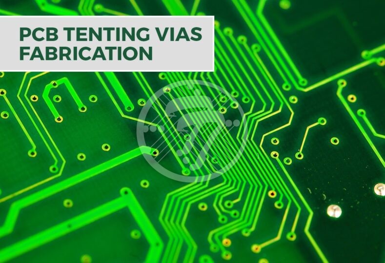
What Is Tenting Via & How It Plays Important Role In PCB Fabrication?

When it comes to establishing connection patterns between the various layers of a board, vias play an extremely important role. Simply put, vias are holes on the PCB without which the connections cannot be formed and therefore the PCB would not work.
They are often covered with different materials as this helps in the twofold process of:
- Helping in conducting electric signals
- Dissipating heat
While this may be thought of as a fairly straight-forward process, the fact is it is quite a specialized process when it comes to PCB fabrication.
Quite often, vias are copper-plated. However it depends on the PCB design whether the holes are covered or exposed. When the via or the hole is fully covered, it is called a masked or a filled via. On the other hand, PCB designers can also use another method called tenting, which is quite popular.
What is tenting via and why is it done in PCB Fabrication?
As its name suggests, tenting via implies creating a tent like shape over the hole. This is done so that the numbers of exposed conductive pads on the PCB are limited.
The process of tenting entails using a solder mask to enclose the opening. Whether or not you should use tenting in the PCB fabrication really depends upon the design of your board.
Below are the benefits and limitations of using tenting in PCB fabrication service:
Benefits of tenting a via
The foremost advantage that tenting vias offers is the protection offered by the solder mask. The tenting creates a barrier that ensures there aren’t any damages to the PCB layers. This is akin to how the solder mask prevents corrosion in the copper traces.
Another advantage of the tenting method is also that the numbers of exposed conductive components are minimized. The exposure of these components can result in corrosion. Tenting also helps in significantly bringing down the possibility of a short on account of the solder bridging. With tenting, you can also rest assured that the paste migration from SMT pads is significantly reduced.
The fact that tenting is a cost-effective method of protecting the vias is an added perk!
Limitations
A major limitation of the tenting process is that with a liquid solder mask, there is always the possibility of breaking of LPI and creating small holes in the tent. In turn, these holes can trap moisture and corrosion can be the natural outcome.
To overcome this limitation, it is important that the vias are left exposed in the prototype stage. That way, any issues can be identified and the traces can be fixed. With covered vias the opportunity to discover these issues is significantly limited.
How to make the decision to tent a via?
Two major aspects go in to decide whether or not you should tent a via. The first, of course is the PCB design and the second is the size of the via.
As a thumb rule, tenting works well with vias of smaller diameters of 12 mil or less. Any via that is above 12 mil in diameter does not lend itself to tenting. If you need to take care of large vias closing it with some kind of fill is a far better alternative.
Tenting is also preferred on account of its lower cost as opposed to mask plugging or epoxy filling. In fact tenting via with a liquid photo-imageable solder mask turns out to be the most cost-effective. However where there are concerns about tenting being loose, epoxy filling is an alternative, even though it comes at a higher cost.
Your PCB fabrication requirements along with tenting via!
With more than 4 decades of experience in PCB Fabrication USA, at TechnoTronix we have the technology and production facility to offer the tenting of vias with the highest degree of accuracy. With our experienced engineers you can rest assured that what you will get is an effective production. Little surprise then that clients across industries rely on us for their PCB fabrication, California requirements. Our ability to deliver, unparalleled quality as well as customer service, is what makes us stand out. Both on-time delivery and price competitive products are our USP. The most important element of our success, however, has been the relationships we have developed with our customers.
If you are looking for full fledged PCB fabrication services from product layout, manufacturing to warehousing and shipping, please explore our PCB fabrication services!


