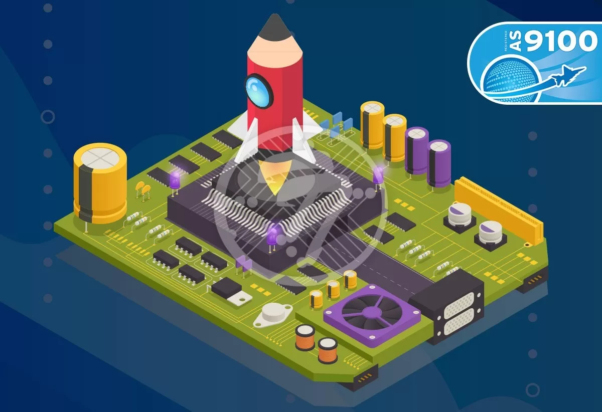
The Significance of AS9100D Certification in Aerospace PCB Manufacturing!

By | Date posted: | Last updated: December 11, 2025
Aerospace PCB Manufacturing

When it comes to mission critical industries, printed circuit boards have to meet rigorous standards. The boards have to be high on reliability, low on maintenance and also have to perform under difficult environmental conditions.

It is for this reason that the AS9100D certification has been instated as a global aerospace manufacturing standard for the aerospace industry. It covers:

  • Aircraft component and materials manufacturers
  • Aircraft part and assembly designers
  • Quality management organizations and other companies that work with aerospace manufacturers

The certification ensures that certified PCB manufacturers and designers work relentlessly towards delivering highest quality PCBs.

What really is the AS9100D certification?

Released in 2009, this standard incorporates all the requirements of ISO 9001 requirements with additional industry specific requirements for aerospace and defense industries. In fact, most aerospace manufacturers and suppliers require compliance with AS9100 as a condition of doing business with them.

Broadly AS9100D focuses on 5 core processes in the aerospace industry, namely:

  • Quality Management Systems
  • Management Responsibilities
  • Resource Management
  • Product Realization
  • Measures of Improvement

By doing this, it ensures there is uniform compliance.
As far as the certification process for AS9100 goes, it is quite extensive and among other things involves:

  • 2 on-site audits
  • Various internal audits
  • Annual surveillance audits, and more

To obtain this certificate, electronics manufacturers have to follow a stringent list of standards over and above the basic ISO 9001 requirements. Not just that, contract manufacturer has to continue to fulfill the accepted standards year on year for renewals. Some of the standards that need to be fulfilled include:

  • Better configuration management than ISO9001
  • Risk management procedures
  • Industry-critical processes
  • Focus on timely delivery
  • Supplier approval process
  • Prevention of counterfeit components

Essentially, the goal of the certification is to demonstrate that the electronic contract manufacturing partner can offer products that meet statutory guidelines as well as customer requirements.

The AS9100D certification is contingent on the following aspects:

  • Product safety – This of course is the key consideration of the certification. Product safety needs to be demonstrated through the entire cycle of the PCB as also high-temperature applications.
  • Risk Based Thinking – Risk of course needs to be factored into all products including PCB boards. With rules around risk management becoming more stringent, proactive steps need to be taken to remain compliant.
  • Counterfeit Parts Prevention – The latest certification includes a whole lot of clauses that ensure that the use of fraudulent products is identified and stopped.
  • Human Factors – Under this certification, human failures are seen as a part of the failure of the system and it therefore offers an opportunity to improve the overall process.

Advantages of AS9100D certification in aerospace PCB manufacturing

With an AS9100D certification, you can rest assured that the contract manufacturer is committed to providing high-quality aerospace electronics PCB assembly & design. Some of the advantages offered include:

  • Customer Satisfaction – Whether you are looking at prototypes or full production runs, with an AS9100D certification you can be assured of complete satisfaction whether it is to do with PCN quality and its adherence to stringent quality standards or that the boards will be delivered on time.
  • Optimal Costs – With the AS9100D certification offering continuous improvement to the manufacturing operations, what it also brings is cost-effective price points.
  • Turnaround times – The processes so honed, offer quick turnaround times that make go-to-market that much easier.

Keeping up with AS9100 certification

Once electronics manufacturing companies earn the certification, they need to go through regular renewals. This ensures that they are complying with revisions if any. Recertification audits ensure that compliance is fully followed. While the recertification audit verifies compliance with all clauses of the standards, surveillance audits only review a sample of the clauses.

To sum up

With AS9100D Certification, you can rest assured that your Aerospace PCB Assembly will come with:

  • Improved product and process reliability
  • On-time delivery
  • Increased efficiency, reduced waste, better resource utilization
  • Improved bottom-line

Doing business with an AS9100D certified company will help you achieve a reliable product, better performance and efficient ways of working. Clearly then, the certification is the defining factor that stands between financial success and costly mistakes.

As an AS9100D certified PCB manufacturer, we combine state-of-the-art technology with our advanced engineering to deliver unparalleled quality aerospace PCB manufacturing services. With our four decades of experience, you can rest assured that we are cognizant of the industry’s best practices and will keep you ahead of the curve. Visit to know more about aerospace electronics PCB assembly & design or feel free to contact us. Also, you can drop an email to us at [email protected] or call us on 714/630-9200.

Challenges & top considerations to make your high-speed board design project successful!

By | Date posted: | Last updated: December 11, 2025
High-Speed Board Design

Two decades ago, if you spoke of high-speed data rate, you were in all probability referring to 3 Gbps. Today, of course, engineers can be dealing with as much as 25Gbps. While we are pushing for faster rates, we are also parallelly making smaller devices given the trend of miniaturization.

With high speed also come a number of challenges, primary among them being interference. In fact the faster the data rates, the harder it can get to protect the integrity of signals.

Making your high-speed board design project success, therefore, involves paying attention to a number of factors.

Here are some of the aspects to watch out for High-Speed Board Design:

Have a plan in place

This might sound like an obvious thing to do, but the fact remains that without a proper plan in place you are likely to suffer a whole lot of setbacks. The plan needs to include aspects such as:

  • Having a visual diagram for the sub-circuits and return current.
  • Knowing the frequency and fastest rise time of each signal.
  • Having a plan to meet requirements for differential signals, controlled impedance and more.
  • Documenting voltage and power requirements.

Document details of your board stackup

It is important to determine which material you will be using for the board and what are the specific constraints that need to be followed in terms of the design rules. FR4, for example, works well when you are working with speeds < 5Gbps. When it comes to between 5-25 Gbps clock speeds, Nelco, SI or Megtron work well. For high-speed designs, Rogers as a material is known to work well. Once the PCB material has been chosen, layer stackup strategies need to be kept in mind. Some of these include:

  • Placing a signal layer adjacent to a plane layer
  • Routing high-speed signals on the inner layers of the board
  • Using multiple ground planes to lower reference impedance.

Power and Ground Planes

The ground plane should not be split with any routed signals. Split it can lead to EMI and signal timing issues. In case a ground plane has to be split, a 0 Ohm resistor needs to be added.

Keeping size of land patterns minimum

With high-speed designs since the board real estate is at a premium, you need to save space. To this end, the minimum oversize of the pads should be kept at 0-5% of the size of the component pins. Also, the less the space given to vias, the more room there is for differential pairs, vias and more.

Route Signals for Maximum Shielding Benefits

To ensure that signals do not interfere with each other or with any component, some of the guidelines to be followed include:

  • Ensure you do not keep long, parallel signals
  • Maintain distance between signal traces
  • Route signals orthogonally

Path for Current Return

Using vias to return currents to their termination is recommended. Ensure also that the vias are impedance matched, differential vias. Return vias also need to be placed close to signal vias.

3W Rule

The 3W rule comes in handy to minimize coupling. The rule states that the separation between traces must be equal to three times the width of a single trace from center to center.

20H Rule

To prevent coupling between power and ground planes, it is advisable to sue the 20H rule. It states that the power plan must be made 20 times smaller than the dielectric thickness between adjacent power & ground planes.

General Routing Guidelines

When it comes to routing guidelines, the following tips will come in handy:

  • Avoiding 90-degree angle bends in your traces.
  • Length match tuning in the PCB design software is necessary.
  • Designing transmission lines with the use of microstrip or stripline traces is imperative.

To sum up

Overall arming yourself with strategies and knowledge to combat issues such as interference can go a long way in maintaining integrity of signals. Choosing the right electronics contract manufacturer who has the necessary experience, expertise and access to industry best practices is something that you must do in order to make your high-speed design successful.

We have over 4 decades of experience in providing innovative high-speed PCB design & manufacturing services. We take an extra step to reach out to your exact PCB manufacturing requirements, high-quality standards, and a strong customer support service to provide quick turnarounds and on-time delivery to our customers. In case you have any questions, please feel free to contact us via email at [email protected] or call us on 714/630-9200.

The Importance of FCT Testing in PCB Manufacturing & Assembly!

By | Date posted: | Last updated: December 11, 2025
FCT Testing

While it is important to stick to the highest quality standards in the process of PCB manufacturing, what is equally important is that you ensure that your board will operate as envisioned. This requires undertaking a set of tests at various stages namely prototyping, manufacturing as well as assembly.

PCB functional testing (FCT testing) comprises a whole range of tests that check for proper functioning of the board. Oftentimes, the manufacturer may also need to modify the PCB design for FCT in order to facilitate PCB functional testing. As long as the manufacturer understands your device’s functional requirements as well as your testing requirements, there will not be too many requirements for sending the design files back and forth. A cloud-based system for data access of course works best.

Let us look at PCB Functional Testing (FCT Testing) in some detail:

Simply put, PCB functional testing refers to a comprehensive testing regimen that determines that a manufactured board is ready to serve its purpose. The goal of PCB functional testing is to identify any defects that could impact its reliability. The defects could be by way of any missing components or as simple as any opens or shorts. PCB Functional testing, therefore, entails a wide variety of tests including but not limited to:

  • Visual Inspections
  • In-Circuit Tests
  • Flying Probe Tests
  • Bench Tests

Above everything else, PCB functional testing (FCT Testing) offers a comprehensive view of signal behavior. Some of the potent signal issues that can be identified through a PCB functional test include:

  • Power integrity issues: PCB functional testing can bring to light any issues such as jitter, low frequency noise, and more.
  • Signal distortion: Signal distortion, Skews and other such behavior can be identified through comprehensive functional testing.
  • Incorrect voltage: Incorrect Voltage can often be a result of a missing or incorrect component.

Comprehensive PCB functional testing involves building a custom test fixture. While this comes at a cost, with high volume manufacturing runs, the cost tends to quickly amortize itself, especially as it guarantees high quality

The Benefits of PCB Functional Testing (FCT Testing) Methods

  • Manual inspections – They are used to verify various aspects of the printed circuit board assembly process.
  • Automated Optical Inspection – It can be used to check issues such as:
    • Shorts
    • Any violations in spacing
    • Drilled hole breakout
    • Solder Paste Application
    • Location and orientation of components
  • X-Ray Inspection – X-Ray inspection can be used to examine components such as BGAs for solder defects.

Some of the systems that can undertake functional testing include:

  • Flying Probe Test: It can detect improper solder connections as also include some limited functional testing.
  • In-Circuit Test (ICT): This system works fast as also runs sophisticated functional tests. However, it isn’t used for low volume production as it is time-consuming and expensive.
  • CableScan: This relies on connectors as opposed to test points. It can search for assembly issues such as improper solder connections while also running functional test signals

Collaborating with the experienced PCB manufacturer

Collaborating early in the PCB design stage with the manufacturer is a great way to ensure the comprehensive testability of the board. With many PCB designs being put on hold before manufacturing, this is a great way to improve turnaround time. It’s important to check that the board complies with the manufacturer’s DFM recommendations and testing capabilities.

It is also important to evaluate that the PCB manufacturer offers the following services:

  • They have experienced test engineers that can develop hardware and software for functional testing, as also test fixtures and structures.
  • They have sophisticated testing equipment for a wide variety of testing such as flying probe tests, ICT and manual testing procedures.
  • They have existing relationships with component manufacturers.
  • They thoroughly document testing results.

To Sum Up

Clearly then, the abilities of the local electronics contract manufacturer are imperative to the success of the circuit board build. Done correctly, PCB functional testing is the most comprehensive testing regimen for determining whether a manufactured board is reliable for your purpose or not. Functional testing is integral to eliminating any errors that may crop up during the production phase, while also helping to reduce cost.

TechnoTronix is an ISO 9001:2015 certified company who delivers one-stop PCB manufacturing services with specialized support, reliable testing, and multi-functional features. Our consistent quality and quick turnaround time captivate us to our customers, who look on us as a one-stop-shop for all their PCB requirements.

If you have any requirements regarding our PCB manufacturing or need urgent assistance, contact us at [email protected] or call us on 714/630-9200.

Top things you need to know about the Rigid-Flex PCB Manufacturing Process!

By | Date posted: | Last updated: December 11, 2025
Rigid Flex PCB Manufacturing Process

Rigid-flex PCBs are extremely popular as they combine the characteristics of rigid as well as flexible PCBs. Essentially, they layer flexible circuit substrates inside rigid circuit board materials. What it offers, therefore, is the stability and strength of rigid PCBs along with the versatility of flexible circuits. The combination of rigid-flex PCB manufacturing opens a wide range of possibilities when it comes to complex and challenging designs. What it also offers is improved service reliability and performance.

Rigid-Flex circuit boards find wide use in commercial and industrial applications including but not limited to:

  • Military
  • Aerospace
  • Digital Cameras
  • Cell Phones
  • Pacemakers
  • Barcode scanners and more

Advantages of Rigid-Flex PCBs

Some of the specific advantages that rigid-flex PCBs offer include:

  • Stability – With their structure comprising of interchanging layers of rigid and flexible PCBs they offer mechanical stability. They also lend themselves to easy installation in small spaces.
  • Reliability of connections – Rigid-flex PCBs offer increased stability as well as polarity. This leads to reliable connections.
  • Cost effectiveness – Rigid-flex PCBs are extremely cost-effective and ensure that your project is viable.
  • High-density applications – With miniaturization and high-density applications growing in popularity so is the use of rigid-flex PCBs.
  • High shock and vibration resistance – Rigid flex PCBs are resistant to shock and vibration and find a place in a wide variety of applications.

Rigid-Flex PCB Design Guidelines

While the advantages of rigid-flex PCBs are well-documented, there are several design guidelines that need to be followed when it comes to manufacturing these PCBs. These include:

1. Determine The Number of Layers

Rigid-flex PCBs are made of alternating layers of flexible and rigid PCB Material. It is therefore important to figure out the exact layer count that is required. It is prudent to consult your electronics contract manufacturer early to ensure that all the requirements can be met.

2. Heat Sinking

Due importance needs to be given to having a heat dissipation mechanism in place. In the absence of it, the device performance can be impacted, and it may also result in damage to the device. The PCB needs to facilitate heat sinking.

3. Material Layup

Layup of materials is yet another crucial factor. This includes checking for:

  • The UL flammability rating
  • Minimum bend radii needed
  • RoHS certification
  • Impedance control
  • Mechanical considerations, and more.

Material layup, in turn, impacts both cost as well as manufacturability.

Steps Involved in Rigid-Flex PCB Manufacturing Process

The rigid-flex PCB manufacturing process involves the following steps:

Base Preparation

This involves preparation of the laminate. The laminate, in turn, features a copper layer. If the copper contains anti-tarnish, it needs to be removed by immersing it in acid solution.

Circuit Patterns / Structure

Through a process of either photo imaging or screen printing, circuit patterns are generated.

Circuit Pattern Etching

Etching the circuit pattern is largely done by spraying a solution over the circuit pattern or dipping the laminate in an etching solution. Etching is then undertaken on both sides of the circuit pattern.

Drilling Holes

Holes are next drilled using lasers. Laser drilling, in turn, assures precision as well as minimizes waste.

Through-hole Plating

Copper is deposited into the drilled holes and plated with a chemical. This step is crucial to create electrical interconnections.

Coating Etch-Resist and stripping

This step involves applying a photosensitive etch-resist coating on the substrate. The chemical resist applied to the plated through-hole is next stripped.

Cover lay Application

A cover lay is applied to the PCB to protect it from harsh environmental conditions. The coverlay material is screen printed onto the surface of the circuit board and exposed to UV.

Cutting the Flex

The individual flex board is now cut from the production panel with extreme caution and precision.

Lamination

In this step, the flexible printed circuit boards is laminated between the rigid sections.

Electrical Testing and Verification

Electrical testing and verification are the final step that ensures circuit performance and quality.

With the above steps you can rest assured that you will get a performance-driven rigid-flex PCB. The important bit is to choose a contract manufacturer that specializes in the fabrication of rigid-flex PCBs, who can understand your bespoke requirements and deliver accordingly.

As a leading rigid-flex PCB manufacturer, we are fully equipped to handle your PCB manufacturing requirements. With over 4 decades of experience in rigid-flex PCB manufacturing as well as assembling PCBs with differing levels of complexities, our team of experts & state-of-the-art equipment ensures that all our PCBs meet the industry standards of quality.

In case if you have any questions or queries regarding our rigid-flex PCB manufacturing services, please feel free to contact us via email at [email protected] or call us at 714/630-9200.