What is PCB cloning? How does it work, and what are its advantages?


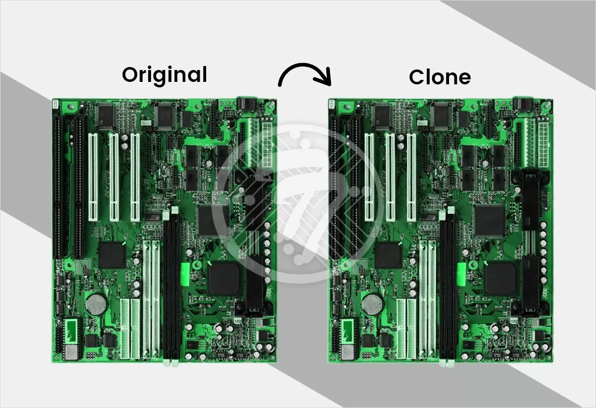
Also referred to as PCB duplication, PCB cloning is a reverse engineering technology that is applied in order to create copies of existing PCBs. It ensures that you can create the exact design of the PCB without going through the laborious design process. It therefore is extremely effective when it comes to saving time as well as cost.
With electronic gadgets evolving continuously, it is hard to use traditional R&D methods to keep pace. Reverse engineering is therefore a powerful option. Not only does PCB cloning extend the life of a device when components become obsolete, it also helps you modify existing designs to meet your bespoke requirements.
How does PCB cloning work?
Done by way of a simple, automated process, the starting point for PCB cloning is for you to have the detailed bill of materials (BOM) as well as the circuit schematics. The steps involved in the cloning process are as under:
- Ensure all active components are removed from the PAD hole & the tin. An ultrasonic is next used to clean the board. The empty board is now scanned.
- Launch Photoshop & copy the scanner to the program.
- A paper yarn can be used to polish the board. The board is next kept on the scanner & Photoshop is re-launched.
- Next the picture is saved as a BMP file.
- Convert the BMP file into PROTEL. Open PROTEL99 & create a PCB file. CAD needs to be imported next and the file saved. 2 levels are to be generated with the PROTEL file.
- Open the CAD files. Next copy the component package into the CAD using the PCB image as reference. Next ensure that the pads & vias are placed correctly. Arrange the pads as per their sizes.
- Next a line needs to be drawn on the top layer & the devise needs to be installed. This needs to be followed by deleting the silkscreen layer.
- Convert the PCB to PROTEL & integrate the diagrams.
- The next step involves printing the layers on a film and putting the film on the PCB.
- Test the cloned PCB.
Advantages of PCB cloning
PCB cloning offers a wide variety of benefits. Some of these include:
Optimizes time and cost
While normally PCB manufacturing is time-consuming as well as costly, PCB cloning helps you in both these aspects. Besides not having to work on the design, it also ensures that you save on PCB testing as well as the creation of PCB prototypes since the original design is well-established.
Simplifies production
It makes the production process simple as manufacturers can reverse engineer innovative designs. With the automated process the entire production process is streamlined. It also helps automate manufacturing processes & saves time & money that come with manual labor. It also ensures production of high-performance & long-lasting boards.
Improved scalability and freedom
It offers flexibility to companies to be adaptable throughout the manufacturing process and to create boards that meet the needs of the consumers. Also, it lends itself to scalability as a large number of boards can be produced from a single PCB design.
Building Customer Friendly Products
With cloning of PCBs engineers build customer-friendly products by reverse engineering the current impactful PCB designs.
Offers Production Flexibility
With PCB Cloning you can use a single design to mass manufacture products.
Consistency in performance
The cloned boards offer consistency in performance since the design has already been tried & tested.
Improves timelines
In a milieu where competitive advantage is derived from quick time-to-market, PCB cloning brings a major benefit. The process is now not only simple but extremely short too.
To sum up
To sum up, PCB cloning ensures that the process is easier, its cost is lower & that PCB production capacity is enhanced. It is no surprise then that manufacturers prefer cloning as opposed to constructing a PCB schematic from scratch.
The one thing to keep in mind though when it comes to PCB Cloning is the issue of copyright as it protects the interest of the original designer.
Technotronix provides a one-stop solution for PCB manufacturing services with specialized support, reliable testing, and multi-functional features. In case if you have any questions, please feel free to contact us via email at sales@technotronix.us or call us at 714/630-9200.