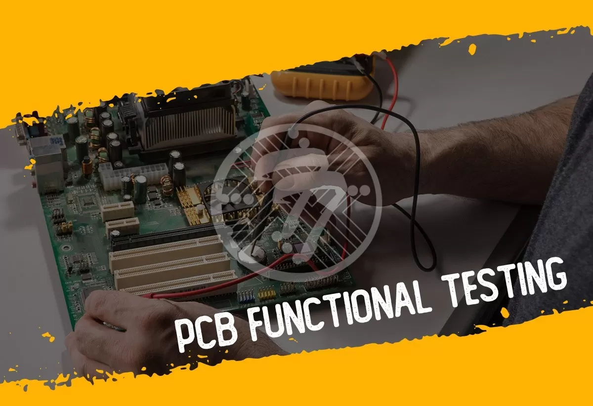
The Importance of FCT Testing in PCB Manufacturing & Assembly!

By | Date posted: | Last updated: December 11, 2025
FCT Testing

While it is important to stick to the highest quality standards in the process of PCB manufacturing, what is equally important is that you ensure that your board will operate as envisioned. This requires undertaking a set of tests at various stages namely prototyping, manufacturing as well as assembly.

PCB functional testing (FCT testing) comprises a whole range of tests that check for proper functioning of the board. Oftentimes, the manufacturer may also need to modify the PCB design for FCT in order to facilitate PCB functional testing. As long as the manufacturer understands your device’s functional requirements as well as your testing requirements, there will not be too many requirements for sending the design files back and forth. A cloud-based system for data access of course works best.

Let us look at PCB Functional Testing (FCT Testing) in some detail:

Simply put, PCB functional testing refers to a comprehensive testing regimen that determines that a manufactured board is ready to serve its purpose. The goal of PCB functional testing is to identify any defects that could impact its reliability. The defects could be by way of any missing components or as simple as any opens or shorts. PCB Functional testing, therefore, entails a wide variety of tests including but not limited to:

  • Visual Inspections
  • In-Circuit Tests
  • Flying Probe Tests
  • Bench Tests

Above everything else, PCB functional testing (FCT Testing) offers a comprehensive view of signal behavior. Some of the potent signal issues that can be identified through a PCB functional test include:

  • Power integrity issues: PCB functional testing can bring to light any issues such as jitter, low frequency noise, and more.
  • Signal distortion: Signal distortion, Skews and other such behavior can be identified through comprehensive functional testing.
  • Incorrect voltage: Incorrect Voltage can often be a result of a missing or incorrect component.

Comprehensive PCB functional testing involves building a custom test fixture. While this comes at a cost, with high volume manufacturing runs, the cost tends to quickly amortize itself, especially as it guarantees high quality

The Benefits of PCB Functional Testing (FCT Testing) Methods

  • Manual inspections – They are used to verify various aspects of the printed circuit board assembly process.
  • Automated Optical Inspection – It can be used to check issues such as:
    • Shorts
    • Any violations in spacing
    • Drilled hole breakout
    • Solder Paste Application
    • Location and orientation of components
  • X-Ray Inspection – X-Ray inspection can be used to examine components such as BGAs for solder defects.

Some of the systems that can undertake functional testing include:

  • Flying Probe Test: It can detect improper solder connections as also include some limited functional testing.
  • In-Circuit Test (ICT): This system works fast as also runs sophisticated functional tests. However, it isn’t used for low volume production as it is time-consuming and expensive.
  • CableScan: This relies on connectors as opposed to test points. It can search for assembly issues such as improper solder connections while also running functional test signals

Collaborating with the experienced PCB manufacturer

Collaborating early in the PCB design stage with the manufacturer is a great way to ensure the comprehensive testability of the board. With many PCB designs being put on hold before manufacturing, this is a great way to improve turnaround time. It’s important to check that the board complies with the manufacturer’s DFM recommendations and testing capabilities.

It is also important to evaluate that the PCB manufacturer offers the following services:

  • They have experienced test engineers that can develop hardware and software for functional testing, as also test fixtures and structures.
  • They have sophisticated testing equipment for a wide variety of testing such as flying probe tests, ICT and manual testing procedures.
  • They have existing relationships with component manufacturers.
  • They thoroughly document testing results.

To Sum Up

Clearly then, the abilities of the local electronics contract manufacturer are imperative to the success of the circuit board build. Done correctly, PCB functional testing is the most comprehensive testing regimen for determining whether a manufactured board is reliable for your purpose or not. Functional testing is integral to eliminating any errors that may crop up during the production phase, while also helping to reduce cost.

TechnoTronix is an ISO 9001:2015 certified company who delivers one-stop PCB manufacturing services with specialized support, reliable testing, and multi-functional features. Our consistent quality and quick turnaround time captivate us to our customers, who look on us as a one-stop-shop for all their PCB requirements.

If you have any requirements regarding our PCB manufacturing or need urgent assistance, contact us at [email protected] or call us on 714/630-9200.

Top things you need to know about the Rigid-Flex PCB Manufacturing Process!

By | Date posted: | Last updated: December 11, 2025
Rigid Flex PCB Manufacturing Process

Rigid-flex PCBs are extremely popular as they combine the characteristics of rigid as well as flexible PCBs. Essentially, they layer flexible circuit substrates inside rigid circuit board materials. What it offers, therefore, is the stability and strength of rigid PCBs along with the versatility of flexible circuits. The combination of rigid-flex PCB manufacturing opens a wide range of possibilities when it comes to complex and challenging designs. What it also offers is improved service reliability and performance.

Rigid-Flex circuit boards find wide use in commercial and industrial applications including but not limited to:

  • Military
  • Aerospace
  • Digital Cameras
  • Cell Phones
  • Pacemakers
  • Barcode scanners and more

Advantages of Rigid-Flex PCBs

Some of the specific advantages that rigid-flex PCBs offer include:

  • Stability – With their structure comprising of interchanging layers of rigid and flexible PCBs they offer mechanical stability. They also lend themselves to easy installation in small spaces.
  • Reliability of connections – Rigid-flex PCBs offer increased stability as well as polarity. This leads to reliable connections.
  • Cost effectiveness – Rigid-flex PCBs are extremely cost-effective and ensure that your project is viable.
  • High-density applications – With miniaturization and high-density applications growing in popularity so is the use of rigid-flex PCBs.
  • High shock and vibration resistance – Rigid flex PCBs are resistant to shock and vibration and find a place in a wide variety of applications.

Rigid-Flex PCB Design Guidelines

While the advantages of rigid-flex PCBs are well-documented, there are several design guidelines that need to be followed when it comes to manufacturing these PCBs. These include:

1. Determine The Number of Layers

Rigid-flex PCBs are made of alternating layers of flexible and rigid PCB Material. It is therefore important to figure out the exact layer count that is required. It is prudent to consult your electronics contract manufacturer early to ensure that all the requirements can be met.

2. Heat Sinking

Due importance needs to be given to having a heat dissipation mechanism in place. In the absence of it, the device performance can be impacted, and it may also result in damage to the device. The PCB needs to facilitate heat sinking.

3. Material Layup

Layup of materials is yet another crucial factor. This includes checking for:

  • The UL flammability rating
  • Minimum bend radii needed
  • RoHS certification
  • Impedance control
  • Mechanical considerations, and more.

Material layup, in turn, impacts both cost as well as manufacturability.

Steps Involved in Rigid-Flex PCB Manufacturing Process

The rigid-flex PCB manufacturing process involves the following steps:

Base Preparation

This involves preparation of the laminate. The laminate, in turn, features a copper layer. If the copper contains anti-tarnish, it needs to be removed by immersing it in acid solution.

Circuit Patterns / Structure

Through a process of either photo imaging or screen printing, circuit patterns are generated.

Circuit Pattern Etching

Etching the circuit pattern is largely done by spraying a solution over the circuit pattern or dipping the laminate in an etching solution. Etching is then undertaken on both sides of the circuit pattern.

Drilling Holes

Holes are next drilled using lasers. Laser drilling, in turn, assures precision as well as minimizes waste.

Through-hole Plating

Copper is deposited into the drilled holes and plated with a chemical. This step is crucial to create electrical interconnections.

Coating Etch-Resist and stripping

This step involves applying a photosensitive etch-resist coating on the substrate. The chemical resist applied to the plated through-hole is next stripped.

Cover lay Application

A cover lay is applied to the PCB to protect it from harsh environmental conditions. The coverlay material is screen printed onto the surface of the circuit board and exposed to UV.

Cutting the Flex

The individual flex board is now cut from the production panel with extreme caution and precision.

Lamination

In this step, the flexible printed circuit boards is laminated between the rigid sections.

Electrical Testing and Verification

Electrical testing and verification are the final step that ensures circuit performance and quality.

With the above steps you can rest assured that you will get a performance-driven rigid-flex PCB. The important bit is to choose a contract manufacturer that specializes in the fabrication of rigid-flex PCBs, who can understand your bespoke requirements and deliver accordingly.

As a leading rigid-flex PCB manufacturer, we are fully equipped to handle your PCB manufacturing requirements. With over 4 decades of experience in rigid-flex PCB manufacturing as well as assembling PCBs with differing levels of complexities, our team of experts & state-of-the-art equipment ensures that all our PCBs meet the industry standards of quality.

In case if you have any questions or queries regarding our rigid-flex PCB manufacturing services, please feel free to contact us via email at [email protected] or call us at 714/630-9200.

Everything you Need to Know About PCB V-Scoring!

By | Date posted: | Last updated: December 11, 2025
PCB V-Scoring

PCB V-scoring is a form of PCB panelization that allows you to both fit multiple PCBs onto a single manufactured board and allows you to separate the boards after assembly. It derives its name from the fact that it involves cutting a “V” shaped groove at the top and bottom of the PCB.

In order to V-score a PCB, what is required is a specialized scoring tool with a top and bottom blade.

The Requirement for PCB V-scoring

V-scoring is required to make the printed circuit board assembly process efficient. The process of V-scoring ensures that the assembled boards can be separated using minimal pressure.

Importantly, V-scoring helps with the following:

  • Making efficient use of the board space.
  • Reducing manufacturing cost by making several PCBs on one board. It also helps with putting two or more related circuits on the same assembly that aids in efficient sub-assembly. Depaneling machines are also relatively inexpensive. Besides, they are portable and not high on maintenance.
  • Saves time as you can easily separate parts from a completed assembly. The process of V-scoring allows you to put components on each section of the board in a single run. Later you can simply separate the boards making the PCB assembly process both cost as well as time-efficient.

Challenges of PCB V-Scoring

  • V- scoring is restrictive in terms of panel design. V-groove isn’t the best option for designs where the components are too close to the edge.
  • It also necessitates a clearance of 0.05 inches between the components and V-grooves. Tall components, particularly, must be placed away so that the cutter doesn’t come in their way. Similarly, components with large connection areas should also be placed away from the groove.
  • V-grooves can impact the structural integrity of the PCB leading to warpage or being caught in the wave-solder machine. Adding jump scoring to the leading and trailing edges of the array, help to strengthen it.

How do you specify PCB V-Scoring?

The PCB V-score can be specified based on the depth of the score or looking at the cross-section.

The standard way to specify the V-score is to cut 1/3rd on top, 1/3rd at the bottom, leaving 1/3rd of the web in the middle. Manufacturers are known to offer a 90 degree and 30 degree score as well. While the ninety-degree score is known to break easier than a 30-degree score, it takes more space on the layout.

General Rules for PCB V-Scoring

The general rules of the thumb for effective PCB V-scoring are as below:

  • The spacing between the boards should be 0 mm.
  • The minimum PCB footprint size for V-scoring is 75mm x 75mm, and the maximum size is 450mm x 1245mm.
  • V-scoring should go straight across the whole board, although floating vertical and horizontal lines are also possible.
  • Spacing between the V-scoring line and the outline of the PCB should be at least 0.35mm.
  • The board thickness of a V-scored board should be at least 0.6mm.

PCB V-SCORE VS. TAB ROUTING PCB PANELS

The choice of V-scoring versus tab routing largely depends on the PCB design. The following factors would come in handy in making the right choice:

  • Shape of the board – V-scoring works well for square or rectangular boards while tab routing lends itself to unusual shapes.
  • Edge components – For edge-hanging components, tab-routing is a far more workable option.
  • Edge Quality – V-scoring results in rough edges. If edge quality is of importance, once again tab-routing will be preferable.
  • Time – Tab routing takes more time and labor to set up. V-scoring, on the other hand, is far quicker.
  • Waste material – V-scoring tends to waste far less material than tab-routing and is therefore more cost effective.

To Sum Up

PCB V-scoring is a major source of cost advantage to electronics manufacturers. It takes away the need for the space needed for routing and therefore offers the ability to add an increased number of rows to the fabrication panel. Wasted laminate is thereby eliminated. Not only does V-scoring save money but also time, as it streamlines the fabrication and processing method.

Technotronix is one of the leading PCB manufacturers in the USA. We have over 4 decades of experience in providing innovative PCB manufacturing services using modern technologies & the latest machinery. We are adhering to strict high-quality standards and compliant with the RoHS (Restrictions of Hazardous Substance) directives. We can fulfil the varied needs of our customers from the simple board to the most complex board for PCB prototype to production. For more information, contact us via email at [email protected] or call us on 714/630-9200.

Leaded Solder vs Lead Free: The biggest debate in PCB manufacturing!

By | Date posted: | Last updated: December 11, 2025
Leaded Solder vs Lead Free

You sure want to stay compliant with RoHS guidelines that restrict the use of hazardous substances in electrical and electronic equipment, lead being one. PCB Manufacturing, however, has been debating the merits of using leaded versus lead free solder for a long time. Let us look at the relative merits of both in detail:

What Are Lead Solders & Lead-free Solders Made of??

Lead solder also referred to as SNPB solder essentially comprises of lead and tin as its base components. Increasingly, the occupational risks of soldering with lead have been highlighted. Essentially, the dust and fumes generated by lead soldering have been found to be toxic when inhaled. Lead based solder is thus a documented health hazard. In 2006, the Restriction of Hazardous Substances Directive (RoHS) was adopted by the European Union (EU).

Lead-free solder has emerged as a replacement of the conventional lead solder. Lead-free solder contains the following substances in varying proportions:

  • Copper
  • Tin
  • Silver
  • Nickel
  • Zinc
  • Bismuth
  • Antimony

Some of the commonly used lead free solders include:

1. Tin-Silver
In such solders, the silver acts as a catalyst as also increases the electrical conductivity of the joint. Tin in this case acts as the base metal which offers strength to the solder. It also acts as a protective agent and reduces the possibility of corrosion.

2. Tin-Copper
The role of copper in the solder is to improve mechanical strength as also the electrical conductivity.

3. Tin-Zinc
The use of zinc goes a long way in lowering the melting point of the solder.

Leaded Solder Vs Lead-free Solder Paste

There are several advantages of using lead solder when compared to lead-free solder.

Advantages of using Lead Solder

Strong joint formation
Lead solder typically offers good electrical conductivity between various metals leading to strong joints.

Ease of use
The advantage with leaded solder is that there is no need for any cleaning agents before its application. The solder paste can be applied directly onto the surface. On heating the molten solder flows into the gaps and once it solidifies it forms a strong bond.

Strong Wetting Property
Since lead solder has a strong wetting property, it is easy for it to flow in narrow spaces.

Disadvantage of Using Lead Solder

The disadvantages of using lead solder includes:

Toxicity
On heating, lead solder produces poisonous gases that can pose a serious threat to life.

Heat dissipation
Lead solder is known for its high thermal resistance. This means heat dissipation is an issue.

Flammability
Given the flammability of lead solder, there is high risk of fire.

Cost
Depending upon the purity level of the solder, the cost of lead solder is also high.

Advantages of using Lead-Free Solder

The advantages of using lead-free solder include:

Low cost
Lead-free solder costs lower than leaded solder and is therefore far more affordable.

Environment friendly
The big advantage with lead-free solder is that is does not produce toxic fumes or waste material and therefore does not contaminate the environment.

Safety
With lead free solder being less combustible, the chances of fire are low.

While lead-free solder joints tend to look different in appearance, joints soldered with lead-free solder paste tend to be reliable. Of course, in order to eliminate soldering defects you need to look at many other factors including but not limited to the temperature, vibration, pre-heating time and throughput and the skill level of the operator. The PCB fabricator’s experience in RoHS material compliance can go a long way in ensuring reliability.

The design layout of the circuit board, and the right component selection also have strong roles to play when it comes to quality control issues. Additionally, the choice of lead-free products needs to be made as per the design parameters. Proper board layout and component selection will ensure that there is no damage to electronic components. This is particularly important as during reflow high temperatures are experienced for extended time periods.

To sum up

Reliability of the final product demands that the solder joints are reliable and that they do not act as a heat intermediary. When making the decision of what kind of solder will work best for your PCB manufacturing project, it is important to consider factors such as:

  • Safety
  • Cost
  • Wiring Requirements
  • Ease of handling, and more.

With a reliable PCB manufacturer you can rest assured that all RoHS material compliance issues are taken care of without sacrificing quality or time to market.

Technotronix is one of the leading providers of Lead-Free PCB manufacturing services to all the dominant industries. Our main strength lies in the extensive experience and skilled team of experts to build Lead-Free and RoHS Compliant PCB Assembly and manufacturing solution. You can drop an email to [email protected] or give us a call at 714/630-9200 to solve your queries or to get a quote.