What is a Heat Sink Printed Circuit Board and its importance in the electrical industry?


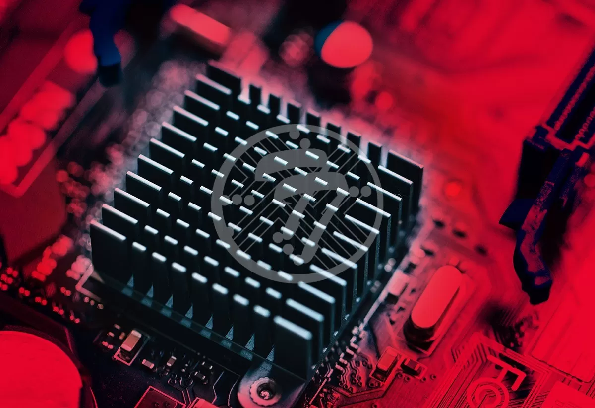
Heat sink technology is of tremendous importance as it allows heat to dissipate and to spread through a circuit. A heat sink PCB is therefore a type of printed circuit board that helps in dissipating high surface temperatures. In fact, heat sink PCBs offer one of the best forms of thermal management. They are ideal for use in applications that generate heat. Most electronics that use heat sink PCBs, therefore, have a longer lifespan.
Why are Heat Sink PCBs important in electronic circuits?
High power devices are known to produce heat. They however have low heat dissipation capability. Some of these devices include:
- Power transistors
- LEDs
- Lasers, and more.
Heat build-up can cause premature failure in the device. Heat sink board, therefore, are the perfect answer.
Benefits of Heat Sink PCBs:
Passive Heat Exchange
Heat sink PCBs can act as passive heat exchangers. With heat dissipated, it leads to improved performance of the device and prevention of device failure.
Maintains Thermal Stability
What heat sinks in PCBs help to do, therefore, is to maintain the thermal stability of the device. In high-performance applications, therefore, their importance cannot be overstated. Additionally, other than heat dissipation they also provide heat during low temperatures. The generation of thermal energy, in turn, allows for the smooth functioning of the circuit.
Spreads heat
In some applications, heat sinks help to spread heat. For example, in case of graphic processors and CPUs of computers, they come in extremely handy to spread heat.
Prevents system failure
In the absence of a heat sink, there is high risk of failure of components. Typically, in mission critical operations, this can be a huge problem.
Types of Heat Sink:
The various types of heat sink are as below:
Active heat sink
Such heat sinks are powered by water pumps and fans, for example, which increase the rate of heat transfer. In some systems these coolers run off the internal power supply. The moving parts of this heat sink do not make it ideal for long-term applications of PCB industrial solutions.
Passive heat sink
Unlike an active heat sink, a passive heat sink does not feature any additional products or processes. In such cases the heat dissipation takes place through the process of convection. Such heat sinks are bigger than active heat sinks.
Types of heat sink based on material:
Aluminum heat sink
Aluminum heat sinks are a popular choice on account of the thermal conductivity of aluminum. In such heat sinks, the heat escapes through thin metal fins. Additionally, the fact, that they aren’t too expensive, adds to their popularity.
Copper heat sink
Copper is known to be a good thermal conductor and has great heat transfer capabilities. However, heat sink PCBs made of copper are more expensive.
Finned heat sink
This type of heat sink is designed in a manner that a large number of thin plates extend outwards from the central block. They offer a high surface area and hence effectively transfer heat away from the components. Typically, such heat sinks use either die-cast or forged models.
Pinned heat sink
This type of heat sink features rods or pins that extend outwards or upwards. While they work well in terms of the overall surface that they offer, they aren’t particularly known for their superior performance.
Heat sink types based on manufacturing techniques
Based on the PCB manufacturing process or techniques, heat sinks can be classified as under:
Stamped heat sink
This heat sink uses stamped metals. Such metals can form a certain shape. Such heat sinks work well for low-power applications.
Bonded heat sink
This kind of heat sink works well for large applications. They are formed by combining separate fins to the base of the heat sink, by either brazing or thermal epoxy.
Skived heat sink
These use fine blocks of metal for manufacturing heat sinks.
Swaged heat sink
These use a cold working forging process for its manufacturing.
Forged heat sink
Such heat sinks make use of compressive forces. This is particularly used in aluminum and copper heat sinks.
Machining heat sink
The machining process is used for manufacturing such heat sinks. However, since it leads to considerable metal wastage, this method is expensive.
To sum up, the characteristics of a good PCB heat sink include:
- It should have a large surface area.
- The heat dissipation needs to correlate with the temperature difference between the device and the ambient temperature.
- Its flat surface should be in contact with the heat source.
- Its design should allow for free flow of air through the fins.
We are one of the leading PCB manufacturers in the USA. we are fully equipped to handle your PCB manufacturing requirements. We take an extra step to reach out to your exact PCB manufacturing requirements, high-quality standards, and a strong customer support service to provide quick turnarounds and on-time delivery to our customers.
In case if you have any questions, please feel free to contact us via email at sales@technotronix.us or call us on 714/630-9200.