Reinvent Multilayer PCB Manufacturing with additive manufacturing!


When it comes to PCB Manufacturing, particularly multilayer PCB manufacturing, the technology that is currently in place, is in many respects not too efficient. Not only is it time consuming, the biggest issue is that it is not foolproof when it comes to avoiding errors.
The big relief has come in the form of additive manufacturing, where it has become far easier to create complex, multilayer PCBs. This technology allows for creating high-density boards which work well especially given the current trend of miniaturization of electronic products.
Before we look at additive manufacturing in some detail, it will be worthwhile to look at some of the issues being faced when it comes to manufacturing multilayer PCBs via the traditional methods.
Issues plaguing the traditional multilayer circuit board manufacturing methods:
Time Consuming
First up, the traditional method is time-consuming. This is largely on account of the fact that there isn’t any significant automation. For an industry where turnaround times are a critical source of competitive advantage, no marks for guessing, that this comes with its own set of problems. Especially, if you are dealing with high-density PCBs, the time taken for PCB fabrication, as also its cost shows a substantial increase.
Material Wastage
Traditional PCB fabrication also comes with a significant amount of wastage of material. From a cost standpoint also this results in less than optimal costs.
Use of hazardous material
At a time where stopping environmental degradation is the need of the hour, traditional PCB Fabrication processes use a whole lot of hazardous chemicals that cause significant environmental damage.
What additive manufacturing effectively does, is to mitigate each of the above risks and offer tangible benefits through 3D printing.
Additive manufacturing process for multilayer PCB manufacturing –
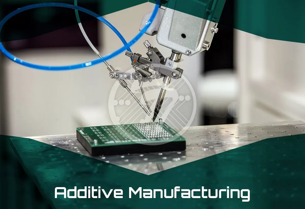
An additive manufacturing process that employs 3D printing of PCBs, essentially uses a layer-by-layer printing process to produce multilayer PCBs.
We do have additive manufacturing processes that involve printing from silver or copper nanoparticle inks directly to a FR4 substrate. However, this helps in single layer boards where the subtractive etching process is eliminated. When applied to multilayer circuit boards, there is hardly any time or cost saving as compared to the traditional PCB manufacturing process.
What works well when it comes to multilayer PCBs is the process of 3D printing. All you need are superior inkjet printing systems whereby you can opt for a layer-by-layer deposition process. What is of importance here, is that the insulating substrate can also be printed simultaneously. All you then require by way of PCB Assembly, is to add the surface finishing and PCB component placement. You do not have to undergo the drilling process since you are able to print the substrate with mounting holes.
If you look at this multilayer PCB closely, what it really has are traces and vias in a single dielectric layer. The advantage clearly lies in the fact that you do not undergo the geometric constraints that come in traditional multilayer PCB production.
Little surprise then that additive manufacturing is increasingly being used in both, complex PCB fabrication, as well as in creating multilayer PCB prototypes where speed as well as efficiency, is key. The importance of additive manufacturing is also growing on account of the fact that the need for complex, multilayer PCBs is on the increase.
Not only does it work well from the standpoint of quality, from a business perspective too it has a number of advantages, including but not limited to:
- Reduced time of production
- Less material wastage
- Optimal Costs
That it can cater to low-volume, high-complexity multilayer circuit boards, is an added perk! Additionally, with the reduced time of production, the circuit board prototypes can be immediately tested. This by itself offers a number of benefits. Firstly, your time-to-market can be significantly improved and you can gain a competitive edge. If you are a startup and need a minimum viable product to showcase to investors, once again, the importance of this cannot be overstated.
Little surprise then that a lot of industries are benefitting from this new method of multilayer PCB manufacturing. With the fast turnaround enabled by additive manufacturing and engineering changes being easily accommodated, the importance of 3D printing is only slated to grow when it comes to its use by PCB Manufacturers in USA.
Technotronix is one of the leading printed circuit board manufacturers based in the USA. We have over 4 decades of experience in providing innovative multilayer PCB manufacturing services using modern technologies and the latest machinery. We are adhering to strict high-quality standards and compliant with the RoHS quality management system. We are capable to fulfill the various need of our customers from the simple board to the most complex board for PCB prototype to production. This unique additive manufacturing system is reinventing multilayer circuit boards manufacturing. You’ll be able to quickly digitally manufacture multilayer PCBs with complex architectures with lower cost and faster production time. To know more, explore our PCB manufacturing services!