Understanding the PCB Burn-in Testing Process in PCB Manufacturing!

By | Date posted: | Last updated: April 14, 2023
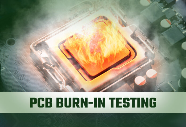
PCB Burn-in Testing

Given the crucial role that printed circuit boards play in the working of appliances, many of them mission-critical, robust testing of PCBs is a key pre-requisite. One such testing method is the PCB burn-in testing also known as stress test, that checks for potential defects early as also helps establish load capacity. The objective of this test is to identify & replace any failed components, early.

In common parlance, burn-in testing detects “infant mortality” or early failure under load. It is thus an integral testing mechanism that helps test load capacity. It also assesses product performance under real world conditions. Its importance particularly in industries such as military, medical, aerospace and more, cannot be overstated.

Broadly burn-in testing involves running the products at elevated voltage and temperature levels as also under power cycling conditions. It could involve:

  • An operating electrical cycle over a time period of 48-168 hours.
  • Thermal cycle with temperatures of 125 degree Celsius for 160 hours.
  • Environmental stress screening.

With Burn-in testing you can:

  • Detect potential failures. The testing therefore plays a huge role in ensuring product reliability.
  • Find out the time to failure. Essentially the testing helps you determine how long a component will last.
  • Measure the mean time between failures.
  • It helps identify defects including but not limited to metallization failures, dielectric failures, conductor failures and electro migration.
  • With manufacturers being able to reduce their returns having found the defects early, it goes a long way in saving time, money & effort.
  • It reduces the huge cost associated with post-production failures including the cost involved with the loss of reputation.

How is Burn-in Testing done?

While the advantages of burn-in testing are immense, how exactly is it done? Essentially, burn-in testing involves operating the product under extremes of temperature & high voltage range for several days so as to detect any defects. During the process, the PCB undergoes electrical as well as thermal testing. Firstly, electric current is passed through the board from between 40-160 hours. The boards are also exposed to temperatures of upto 125 degrees Celsius for 160 hours or longer.

The board that is used for the burn-in test is made out of FR4 flame retardant material. However, when the temperature of the board exceeds 125 degrees Celsius, boards made of ceramic & polyamide are used.

An important aspect to note is that if the board is put to more stress than it is designed to withstand, it can reduce the longevity of the board. Therefore, while it is important to adequately check the board, in case few or no flaws are discovered the test limit can be lowered.

Types of PCB Burn-In testing

The two types of burn-in tests include:

  • Static Burn-in Testing – In such testing the PCB is not in operational mode when it is subjected to high voltage & temperature. This, thus, is a simpler procedure.
  • Dynamic Testing – In this testing the PCB is subject to high voltage & temperature while it is in operational mode. This is largely used for complex PCBs.

As a thumb rule, burn-in is best done at the component level. This is because at that level the cost of testing as well as replacing parts is the lowest. With different components having different limits, it is difficult to conduct burn-in for the board or assembly. This is not to say that it cannot be done, as it helps bring to light issues such as dry solder joints as well as issues with contact.

To sum up

To have the printed circuit board fail a burn-in test is to avoid costly errors at a later date. Especially for mission critical products where you cannot afford to have any failure rate, the importance of a burn-in test cannot be overstated. You sure want to go with a manufacturer who follows the highest protocols when manufacturing the board and also the most stringent measures while testing it. It is important however for the electronic contract manufacturer to follow the specified parameters in the testing as you do not want to subject the electronics to more stress than they are rated for and reduce their lifespan.

Technotronix is an ISO 9001:2015 certified company who provides comprehensive PCB manufacturing services, including specialized support, testing, and multi-functional features. Our commitment to consistent quality and rapid turnaround times makes us a go-to choice for customers seeking a one-stop-shop for all their PCB requirements.

If you have any requirements regarding our PCB manufacturing or need urgent assistance, contact us at sales@technotronix.us or call us on 714/630-9200.

Here’s how to identify the right box-build assembly manufacturer!

By | Date posted: | Last updated: March 28, 2023
Box-Build Assembly Manufacturer

The Electronics box build is precisely constructed to meet a PCB product’s design requirements and safety standards. They include one or more printed circuit board assemblies, interconnecting cables, user interfaces, and other sub-assemblies in a well-fitted box. Many contract manufacturers provide box-build assembly services like system-level assembly, software loading for product configuration, testing, packaging, shipment, and after-sales support. Handling multiple vendors for different services can be time-consuming and expensive. Hence, finding the right box-build assembly manufacturer is crucial for a successful product launch.

Building all the major components of your electronic product on a single shop floor can be highly beneficial. Collaborating with a box-build CM will improve data coordination, hardware compatibility, and system integration. But the capabilities of the service providers vary. It is important to evaluate their expertise, processes followed, the pricing offered, and delivery timelines before signing the contract. Based on the services required, the online quote calculator can assist you in choosing the best CM for your box building.

With the growing demands for miniaturization electronics, packaging of flex PCBs and HDI (High density interconnect) PCBs in compact enclosures largely depends on the efficiency of your CM. The complexity of the box-build assembly can be simple or advanced based on the end product. Fitting a single PCB in a chassis with no additional interfaces can be quite easy. But accommodating multiple PCBs with external connections to display units or other subassemblies may require additional assembly steps. In such situations, an experienced CM can foresee the possible obstacles and suggest preventive actions.

Prerequisites for box build assembly:

To start with a box-build assembly, you have to share certain important design details with your CM. Involving them from the early design stage can be beneficial as they can start working parallelly on their setup readiness. We are listing below the key requirements for a box-build assembly.

  • Product dimension along with its weight
  • Bill of Materials (BoM)
  • Product 3D model using CAD tools
  • Test cases like basic electrical safety testing
  • Golden unit for reference
  • Packaging and shipment guidelines
  • Other design documents like schematics, wire list, and assembly drawings if required

In a box-build assembly, along with the electrical details of PCBs, it is necessary to share the mechanical specifications of subassemblies, cable drawings, connector interface diagrams, etc. A clear understanding of product dimensions is crucial as it impacts the box handling, storage, and delivery requirements. A multi-hierarchical PCB bill of material (BoM) includes both electrical and mechanical lists of components for the complete box assembly. It is necessary to perform top-level system testing before shipping the product to the customers. CM will ask for test procedure documents in such cases. Providing a sample unit for reference can result in a safe box building.

Process of box build assembly:

A box-build assembly consists of PCB assembly, cable construction, custom enclosures, heatsinks or fan assembly for heat dissipation, batteries for power backup, etc. The process starts with the system integration of tested PCBAs with associated circuitry. Verified cables are connected between PCBAs and user interfaces. The mechanical structure is assembled with connectors and brackets as per the design.

A basic visual inspection is conducted to ensure the correct and complete assembly of the box. Memory devices are programmed with setup configurations to boot up the system. Further testing of the overall system is performed as the test documents instruct. Reports are archived and correct labeling of the system is completed. The ready-to-ship products are stored as per the packaging instructions before deployment. The boxes are tracked till delivery to the customer and feedback is obtained.

Advantages of hiring a box-build assembly manufacturer:

There are several benefits associated with a box-build assembly provider. The system integration issues, and debug time can reduce significantly as the whole box is assembled and tested in one single place. Other merits are as follows:

  • Product customization can be done easily along with quality control.
  • Reduced production costs as the components are procured at competitive prices in bulk. Also, eliminating multiple vendor interactions saves time.
  • A robust supply chain ensures a seamless assembly line with minimized downtime. This further improves the production yield.

How to choose the right box-build assembly provider?

As we know the merits of hiring a box-build CM, it is important now to identify the right service provider. Below are the checkpoints to choosing the best box-build assembly manufacturer.

  • The experience of the CM should match the product type you are building. Handling the complexities of the latest technologies is crucial and needs expertise.
  • As box building requires complete knowledge of system integration, the CM should be capable of assembling PCBs, cables, and mechanical enclosures. Adapting to the changes is key in the box-build assembly.
  • Electronic products have to be compliant with various industry standards to assure user safety. This requires your CM to be ISO 9001 certified. Other industry-specific certifications like ISO 13485 for medical electronics and IATF 16949 for Automotives are also required based on the end product.
  • Evaluate the engineering resources of your CM before signing the contract. Component sourcing, design assistance, and testing support should meet your product requirements. You need to have a dedicated support team and a point of contact for all your queries. The CM should have enough resources to handle your build load effectively.
  • Identify the documentation process followed for tracking and issue resolution during the box build assembly process. This is important for quality analysis of the processes followed.
  • The CM should have the latest equipment in the assembly line. All the machines should be calibrated and well-maintained. Based on the product complexity, your CM should be flexible to upgrade the assembly line to meet the delivery requirements.

Conclusion:

Box-build assembly has become popular in the industrial, military, and aerospace sectors. It is commonly used in control panels of manufacturing units. A box-build assembly provider offers diverse services like sub-system assembly, cable assembly, component labeling, enclosure fabrication, firmware configuration, etc. Based on the size and complexity of your product, the above checklist can guide you in finding the right box-build CM.

TechnoTronix excels in providing tailor-made PCB box build assembly services with its fully integrated advanced technologies. In case if you have any questions, please feel free to contact us via email at sales@technotronix.us or fill out the form below to request a free quote now.

GPS PCB BOARD – Design, Functions & Its importance in the modern era!

By | Date posted: | Last updated: March 25, 2023
GPS PCB Board

At one time the importance of big GPS navigators could not be overstated. With the advancement of technology, however, these aren’t required. Instead GPS technology can be integrated into PCBs. Let us take a close look at what a GPS PCB really is:

What is a GPS PCB Board?

Essentially it refers to a printed circuit board, which is integrated with a GPS navigator device. The GPS navigator device, in turn, contains the following:

  • GPS Patch antenna
  • GNSS Antenna
  • Ceramic Patch

The GPS Antenna, in turn, can be of two types- active and passive. The difference between the two is simply the presence & absence of a low noise amplifier. An active antenna is directly placed on the board. The active antenna is known for its high performance on account of the low noise amplifier, which controls the noise. With a passive antenna, the LNA is deployed on the PCB which is designed to decrease the noise in the output. In such cases, however, you need to shield the signal trace from crosstalk & EMI.

GPS Antenna in PCB

Incorporating a GPS antenna into the PCB turns them into a source of mixed signals. Any noise, therefore impacts the signal quality. There is also the possibility that the entire antenna signal is blocked or that it becomes susceptible to ground plane noise.

It is also important to isolate the other components located on the PCB. If adequate isolation is not undertaken, the signal can degrade. The receiver particularly can lower the signals especially when it has an internal antenna. Also, proper shielding is needed to prevent crosstalk between the other components and the receiver.

What is also important is that you undertake filtering so that the GPS signal can be extracted. Introducing a SAW filter between the Low Noise Amplifier & the receiver is seen to be an adequate mechanism. The SAW filter allows filtration of frequencies above 1 GHz.

Grounding and Routing

Proper grounding, shielding, and routing is essential for a GPS enabled device. In the absence of this noise, it could block signals from the GPS receiver.

It helps to create well-functioned blocks in the PCB with their own ground planes. The ground planes, in turn, are routed back to their initial ground state to ensure that there aren’t any ground loops. You need to isolate the GPS receiver and match the network to its ground plane. It can then be connected to the digital ground plane at one point. The RF (Radio Frequency) ground plane comes in handy to ground the data lines.

It is also important to route the antenna traces within a shielded enclave. Burying the antenna traces within an internal printed circuit board layer and placing the matching circuit’s ground planes on either side, is recommended. While the embedded antenna needs to be positioned outside the shield, the battery & other electronics need to be shielded from the antenna.

What are some of the factors to consider in choosing GPS PCB board?

First up, it is important to choose the GPS module or chipset. It is also important to remember that the cost of a GPS simulator is often as high as between $10,000 to $15,000. It is therefore important to factor this cost in.

It is also important to determine if your goal is to use GPS antenna, which is passive or active. With a passive antenna design you have to contend with many complexities, as you need to ensure that there is proper isolation from components. Testing with passive antenna designs is also challenging.

You also need to figure out which antenna element is required. For instance for mobile equipment, you tend to benefit from a patch antenna. A patch antenna receives signals on either side. A chip antenna receives signals along a single axis.

Importantly, you also need to effectively deal with the noise as also have an impedance-controlled PCB.

In terms of PCB design, another aspect to remember is that the RF traces need to be kept on the uppermost layer of the PCB. Also, to reduce inductance, you need to increase the number of inductors.vias. It is also important to place components end-to-end and to avoid track-stubs.

To sum up

To say that GPS enables PCBS have become ubiquitous is to state the obvious. It is important to understand the many issues behind a successful design, it order to ensure that you have an optimal product.

Technotronix provides a one-stop solution for PCB manufacturing services with specialized support, reliable testing, and multi-functional features. In case if you have any questions, please feel free to contact us via email at sales@technotronix.us or call us at 714/630-9200.

PCB AOI: Role of Automated optical inspection in PCB Manufacturing

By | Date posted: | Last updated: March 17, 2023
PCB AOI

The importance of testing in PCB manufacturing cannot be overstated. With PCBs being used for mission critical operations, the integrity & smooth functioning of the PCB is central to the efficacy of the device.

One of the important tests to check whether the PCB has any manufacturing faults is Automated Optical Inspection or what is popularly known as AOI.

What is Automated Optical Inspection (AOI)?

Essentially as its name suggests, it is a machine-based technique that checks the PCB for any potential defects such as:

  • Surface Defects
  • Dimensional Defects
  • Component Placement Defects

With complex circuit boards and boards being manufactured in large quantities, manual checking becomes more & more difficult. AOI therefore has emerged as an important tool to check efficacy of the board at cost effective price points. Let us look at how it really works.

How exactly does AOI work?

Essentially the process works as follows. A first article PCB is manually inspected. Found good, it is established as a “golden” unit. The AOI then learns from this unit what the gold standard is, in terms of various aspects such as component placement, solder joints and more. This information is then stored in its database. The AOI system then compares each new board with this unit & alerts the operators in case of any inconsistency. The AOI system is equipped with high-resolution cameras, which capture a wide array of images, which come in handy for the comparisons. Different equipment works well for different kinds of inspection. So, while solder paste inspection is done by way of laser scanning, an assembly verification system relies on imaging.

Some of the methods that AOI makes use of, include:

Template matching – Simply put, this is a pixel-by-pixel method, where a small template is applied to a large inspection image. Normalized Cross Correlation is then calculated between the template & inspection image.

Object recognition – This method simply relies on a comparison between the ideal image & the captured image

Blob analysis – This involves separating the object from the background & then generating a blob by grouping object pixels.

Advantages of Automated Optical Inspection

AOI offers a wide range of advantages including but not limited to:

Miniaturization

With the increasing trend of miniaturization, the size of PCB components is constantly on the decline and component density is high. In such a scenario, AOI comes in extremely handy in checking for the positional accuracy of components. The advantage with AOI is that it can detect even small deviations in position eliminating chances of a defect.

Versatility

The big advantage with AOI is that it is useful not only in case of PCB fabrication but also in PCB assembly where it helps in checking for aspects such as soldering and polarity. The fact that AOI can be used at any stage makes it an ever so important tool when it comes to inspection efficacy

Programmable lighting

AOI makes it possible to configure light arrays within the inspection software. In turn, this is an invaluable tool that helps in a wide range of defect detection.

Data collection & Retrieval

AOI also helps in collection & retrieval of data which can take different formats such as image, data, text & more.

Cost Advantage

That AOI can help detect any manufacturing defects & save you from costly errors at a later date, makes it an extremely cost-effective process.

Let us also look at some of the defects that AOI can help check. These are on the spectrum of both Fabrication & Assembly.

Fabrication:

  • Shorts
  • Any violations in trace width
  • Spacing violations
  • Excess copper
  • Missing component footprint pads.
  • Drilled hole breakouts in PCB pads

Assembly:

  • Inspection of solder paste.
  • Finished solder joints.
  • Checking the alignment of components
  • Polarity indicators for component orientation.
  • Marking of components
  • Location of fiducials.
  • Labels as well as other markings.

With the ability to capture a wide range of defects, little surprise then that AOI finds wide application. What it offers is both quick & accurate inspection of errors and thereby it ensures high quality PCBs. Right from bare circuit boards to the SMT Assembly line, its importance is therefore ubiquitous.

Technotronix is one of the leading PCB manufacturers in the USA, providing custom, lead-free and RoHS compliant PCB manufacturing solutions. Whether your requirement is for prototypes or large production runs, we have you covered.

Email us on sales@technotronix.us or call us on 714/630-9200 to solve your queries related to our standard PCB services.