How do consumer electronics OEMs pick up their contract EMS partner in the USA for mass production?


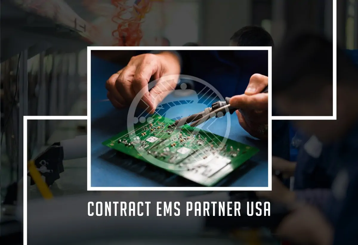
Electronics manufacturing is an exhaustive process and hence most original equipment manufacturers (OEMs) focus primarily on product design and revenue generation. They often outsource supply chain and manufacturing to Electronics Manufacturing Service (EMS) partners. OEMs own intellectual property rights as they work on design innovations and product development. EMS partners offer multiple value-added services like testing, repair, and shipment along with PCB fabrication and assembly services. They are specialized in different production environments like high-mix low volume and low-mix bulk manufacturing. If you are an OEM and looking for a suitable EMS partner in the USA, then this article will provide you with key checkpoints to pick the top service provider for your consumer electronics.
Electronic OEMs can range from a small startup to a large product company. They can deliver products in diverse domains like consumer electronics, the healthcare sector, automotive, aerospace applications, etc. The OEMs have to go through a complete product development lifecycle starting from concept evaluations using prototypes to customer deployment with mass productions.
Multiple driving factors are also influencing the OEM market. For instance, technological trends like 5G, and high-end audio-video solutions have boosted consumer electronics significantly. On the contrary, a shortage of semiconductors has delayed product delivery with long lead times for ICs and other electronic components. So, choosing the right EMS partner is crucial to building successful electronic products and staying ahead in the race.
OEMs generally sell high-volume electronic products to their customers and look for EMS partners offering mass production at reasonable rates. But the OEM product development must go through different phases of its lifecycle and requires EMS support accordingly.
- In the initial concept development stage, your EMS partner should be open to building small-quantity prototypes and adaptable to frequent changes and re-spins.
- After finalizing the design, EMS partners assist in the printed circuit board fabrication and assembly processes. They can source all the components of the product BoM at a cheaper cost as they procure in bulk and from multiple vendor networks.
- EMS partners offer testing and repair services for your assembled products. They can obtain industry-standard certifications based on the end applications. This is mandatory for selling electronic products to your customers.
- With the necessary certifications in hand, you are ready for mass production of your product. Most EMS partners offer additional services like storage, shipment, and after-sales support.
Based on the requirements, OEMs can pick a suitable EMS partner and collaborate. Before interacting with any contract EMS partner, OEMs need to summarize their product specifications, generate a competitive timeline, and make a baseline budget for their project. There are many service providers available in the USA. Identifying the right partner depends on certain key factors. We shall discuss these checkpoints in the following section of the article.
Selection drivers for OEMs to pick their right EMS partner:
- Ensure your product type and specifications matches the EMS partner’s experience and capabilities.
As a consumer electronics manufacturer, your products are built for dedicated services (IPC Class 2). The features may include different technical complexities. So, the EMS partner should have experience in handling consumer electronics design. You can ask for their previous customer references to understand their skills and domain knowledge. - Check if the EMS partner can scale up their production support
As consumer electronics are built for industrial applications, entertainment, communication, or personal usage, they are always in demand. Hence, the required build volume is very high. OEMs have to check if the EMS partner can support mass productions and maintain the required quality. Their technical capabilities and robust supply chain management are crucial in fulfilling bulk orders on time.Checkout how contract manufacturers eliminate the challenges of supply chain management.
- Ask for the geographical location of the EMS partner
For quick delivery of consumer products, it is recommended to hire an EMS partner in the same geographical location as your end market. So, ask for their factory locations. If they are placed nearby, you can have quick site visits during New Product Introduction (NPI) process. - Know the baseline and total cost involved
Go through the quotation and understand each pricing detail clearly. Compare it with your baseline budget and ask for details on any hidden or exorbitant charges. Ask for the total cost involved for all the services including delivery to the customers. Based on the lead time, the pricing may vary. Find out the available options before placing your order. - Decide on component sourcing and supply chain stakeholders
If you want your EMS partner to source all the components, then share the complete BoM and AVL (Approved Vendor List) in advance. Check if they have multiple vendors to procure critical components. EMS partners procure long lead-time components in advance and track the component’s lifecycle. While building consumer electronics, your EMS partner’s supply chain must be efficient and seamless. - Evaluate the company and its team’s competence
Along with the technical capabilities of your EMS partner, do check the strengths and weaknesses of their team. Are they adequately trained to handle your product’s intricacies? Their quality policy and staff’s competence will determine the customer experience of your consumer products. - Ask about NDA and your IP protection
Many OEMs are competing in the consumer electronics industry. It is vital to safeguard your intellectual property from other players. So, ask your EMS partner about their legal policies and sign an NDA agreement before sharing your design. - Get to know about the financial position of the EMS partner
To ensure a long-lasting collaboration with your EMS partner, you need to know their financial status. They should be capable of adapting to market changes. Are they open to procuring new machinery or support with software upgrades if required? These questions can help you to pick a reliable EMS partner.
Conclusion
Consumer electronics is one of the rapidly growing sectors in the electronics industry. An EMS partner must support bulk manufacturing to meet this demand. OEMs have to evaluate the process quality, domain expertise, pricing, timelines, etc. This article provides all the key drivers and assists in selecting the right EMS partner for your successful product build.
We are an ISO 9001:2015 & AS9100 Rev. D Certified company with focus and unique ability to provide you with exactly the PCB manufacturing services you require at the best price! From design and concepts to complete turnkey products, we work our clients to deliver the right PCB industrial solution for aerospace, electronics, Defense & military, telecommunication, medical, renewable energy and more.