
How do plated through holes improve the performance of PCBs?


When it comes to PCB board design, the use of through hole technology is extremely important. With multi board layers, these holes ensure connection between components and conductors. In turn, through hole may be plated or non-plated.
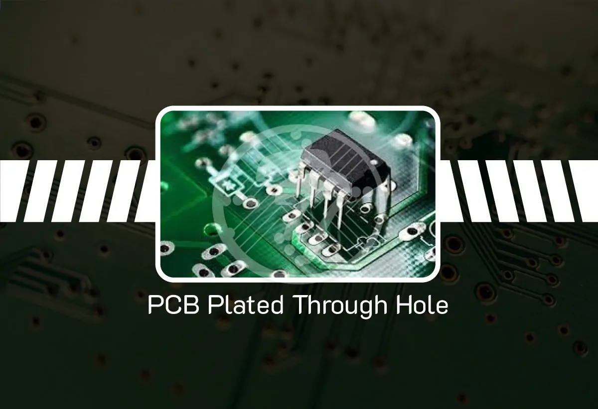
As their name suggests, plated through holes come with a metal coating inside. They are highly in use where electrical connections cannot be compromised and need to have a high degree of reliability. Some applications where plated through holes find application include connectors, switches and ICs.
Non-plated through holes on the other hand, do not have a metal coating on the inside. In such cases the electrical reliability isn’t as high as that of plated through holes. Non plated through holes are known to work well for passive components such as capacitors and resistors.
Improved performance with plated through holes
The big advantages that plated through holes offer, include:
- They enable the flow of current via the PCB’s non-conductive substrate. Hence the current can flow through the components on the other side of the board.
- The added advantage that plated through holes offer is that the hold the components firmly.
- They also ensure that space available is maximized. In fact, plated through holes allow for vertically stacking the custom printed circuit boards. They therefore lend themselves to high component density & hence to miniaturization.
- They offer high amount of electrical conductivity.
- They lend themselves to quicker prototyping as it is easy to solder components on the circuit board.
- They ensure higher power tolerances as well as durability of components.
By contrast, a non-plated through hole, since it doesn’t have conductive plating, does not allow the flow of current through it. It is, however, the design specification of the board that determines whether a plated or a non-plated through hole will be used. If a plated through hole is put in a scenario where a non-plated one should have been put, it will lead to the charge spreading as also weakening of charge. This could even lead to situations such as a short circuit.
It is therefore important to choose the right PCB contract manufacturer as issues related to plated through holes can impact the functionality of the board. An experienced PCB contract manufacturer will be able to offer right solutions. Some of the problems & likely solutions include:
- Blistering & lamination – This occurs on account of poor joint adhesion and can be avoided by maintaining cleanliness. Choosing a conformal coating that is less permeable is also an important solution.
- Roughening of the copper surface – This could lead to blistering. The solution to this lies in checking the humidity in the micro etching machine.
- Insufficient Copper – This leads to plating voids. It therefore needs to be ensured that the quantity of copper is sufficient.
- Long storage times – It is imperative that the boards aren’t stored for long after PTH. It fact after PTH the boards should ideally be finished within 8 hours.
- Plugholes – It is important that the plugholes be done right so that the circuit is not damaged. Aspects to be taken care of include checking the filtering system as also ensuring that there is no panel copper residue or any foreign material on the panel.
To sum up
Plated through holes find extensive application when it comes to multi-layer PCBs. In addition, they are useful in applications where strength of physical connections is key. It is therefore common to witness the use of PTH in aerospace and military applications where durability is a key factor. Plated Through holes also work well for prototyping & testing & therefore goes a long way in ensuring the success of your project.
Non plated through hole (NPTH), on the other hand, works well when it comes to single layer boards.
It is important to make the choice of the right PCB contract manufacturer who is experienced and can ensure that the common issues related to PTH are avoided & the functionality of the board is not compromised. It is important to remember that the design of PTH PCB needs a lot of skill and dexterity. The choice of the right partner can therefore make all the difference.
At Technotronix, we offer comprehensive PCB manufacturing services that come with specialized assistance, dependable testing, and versatile capabilities. If you have any inquiries, do not hesitate to get in touch with us through email at [email protected] or by calling 714/630-9200. We are always happy to help.


