What makes 16-layer printed circuit board manufacturing ideal for complex and dense electronics?

By | Date posted: | Last updated: March 18, 2026
16 layer printed circuit board manufacturing

16-layer Printed Circuit Boards (PCBs) represent the pinnacle of modern electronics, providing unmatched versatility and performance. Composed of 16 stacked layers, these PCBs are essential in powering advanced technologies across various industries. As a leading multilayer PCB manufacturer, we offer insights into the complexities and benefits of these sophisticated PCBs. To learn more about 16-layer printed circuit boards, continue reading this article.

What Are 16-Layer Printed Circuit Boards?

16-layer Printed Circuit Boards, commonly referred to as 16-layer PCBs, are a type of multilayer PCB configuration consisting of sixteen individual layers stacked together. These layers are crucial for handling complex and high-density electronic designs. The stackup of a 16-layer PCB typically includes ten routing layers along with additional layers serving various purposes.

Manufactured using halogen-free materials such as aluminum, CEM, and FR, 16-layer PCBs offer significant advantages in terms of versatility and performance. With a board thickness that can extend up to 7 mm and a maximum finished size of 500 x 500 mm, these PCBs provide ample space for accommodating numerous components and intricate circuitry.

One of the key components of a 16-layer PCB is the prepreg sheets, which act as insulating materials between the copper foil layers. Prepreg, consisting of fiberglass cloth coated with a resin system, ensures proper insulation and prevents signal interference between adjacent layers.

Copper foil sheets constitute the outer layers of the 16-layer PCB stack-up and serve as the primary conductive material for transmitting signals and power throughout the PCB. These copper layers are crucial for establishing electrical connections between components and routing signals across different layers of the PCB.

Additionally, laminate sheets play a vital role in the construction of 16-layer PCBs by providing a substrate for bonding the copper layers. Composed of glass or resin material with copper layers on their surfaces, laminate sheets are used for etching signal layers and inner planes, contributing to the overall functionality and improve performance of the PCB.

What Are the Advantages of 16-Layer PCB Manufacturing?

Here are the advantages of 16-layer (multilayer) printed circuit board manufacturing.

  • High-density feature, ideal for high-speed printed circuit boards.
  • Efficient signal routing and improved signal integrity.
  • Increased functionality by accommodating more components and circuitry.
  • Reduced overall size compared to other PCB types.
  • Lightweight construction due to the elimination of connectors for separate PCBs.
  • Enhanced durability with multiple layers of insulation and bonding materials.

What Are the Applications of 16-Layer PCBs?

The applications of 16-layer PCBs span across a wide range of high-tech industries and specialized fields, owing to their advanced capabilities and versatile design. Some notable applications include:

Satellite Systems:

16-layer PCBs are crucial components in satellite systems, facilitating reliable communication and data transmission in space.

Industrial Controls:

These PCBs are utilized in industrial control systems for monitoring and managing various processes and machinery with precision and efficiency.

GPS Technology:

16-layer PCBs play a vital role in GPS technology, enabling accurate tracking and positioning of networks and devices.

Telecommunications:

They are essential in repeaters for cell phones and communication systems, enhancing signal transmission and amplification for improved connectivity.

Computer Systems:

16-layer PCBs are integral to computer systems, including file servers used for data storage and processing, ensuring seamless operation and reliability.

Medical Equipment:

They are utilized in the medical industry for manufacturing equipment such as heart monitors and X-ray machines, contributing to the advancement of healthcare technology.

Test Equipment:

These PCBs find applications in various laboratory test equipment, providing precise measurement and analysis capabilities for scientific research and experimentation.

Meteorological Departments:

16-layer PCBs are utilized in weather analysis systems deployed by meteorological departments for monitoring and forecasting weather patterns.

Nuclear Detection Systems:

They play a critical role in systems designed for nuclear detection, ensuring accurate and reliable detection of radioactive materials.

Atomic Accelerators:

These PCBs are essential components in atomic accelerators, contributing to the study of particle physics and fundamental scientific research.

What Is the Manufacturing Process of 16-Layer PCBs?

The manufacturing process of 16-layer PCBs involves several key steps to ensure the production of high-quality, high-density printed circuit boards. Here’s an overview of the process:

Material Selection:

The process begins with selecting the appropriate materials for each layer of the PCB. Common materials include prepreg sheets, copper foil sheets, and laminate sheets.

Laminate and Copper Foil Application:

The selected materials are used to create the layers of the PCB. Copper foil sheets serve as the main conductive material for transferring signals and power, while laminate sheets with copper layers are used for bonding on the glass laminates. The signal layers and inner planes are etched on the laminate pieces.

Layer Stacking:

The layers are stacked and bonded together to form the complete PCB. This step requires precision to ensure proper alignment and bonding of the layers. The thickness of the final PCB can vary depending on the specific design requirements.

Drilling and Plating:

Holes are drilled into the PCB for mounting components, and these holes are plated with a conductive material to create electrical connections between layers. This step is crucial for establishing proper connectivity within the PCB.

Etching and Imaging:

The copper layers of the PCB are etched to create the desired circuit patterns. This is typically done using photolithography, where an image of the circuit pattern is transferred to a photosensitive material on the PCB. This step defines the electrical pathways on the PCB surface.

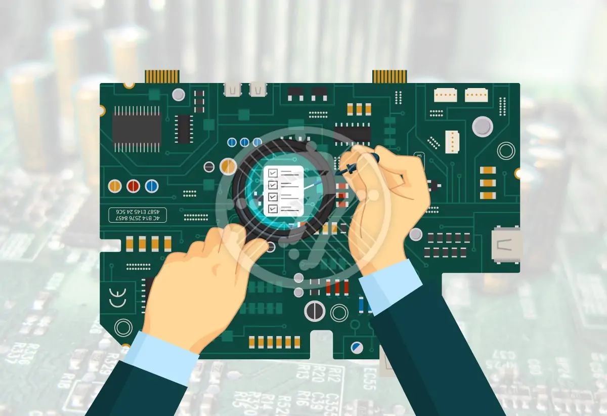
Final Inspection and Testing:

Once the PCB is fully assembled, it undergoes a series of inspections and tests to ensure proper functionality. This can include functional testing, X-ray inspection, burn-in testing, flying probe testing, in-circuit testing, and optical inspection. These tests ensure that the PCB meets the required specifications and performs as expected.

What Are the Challenges and Considerations?

The challenges of manufacturing 16-layer PCBs include:

  • Increased complexity in design and layout, requiring meticulous attention to signal integrity and component placement.
  • Higher manufacturing costs due to complexity and specialized materials.
  • Limited availability of skilled labor and specialized equipment.
  • Risks of manufacturing defects and quality issues, necessitating stringent quality control measures.

Conclusion

In summary, 16-layer PCBs represent a pinnacle of technological innovation, offering unmatched capabilities for a wide range of applications. As technology continues to advance, these PCBs will remain at the forefront, shaping the future of electronics with their advanced features and reliability.

Why Choose Technotronix as 16-layer PCB Manufacturer?

Looking for top-tier quality and precision in PCB manufacturing? Look no further! At Technotronix, our team specializes in manufacturing 16-layer PCBs with unparalleled expertise and attention to detail. Whether you’re in aerospace, telecommunications, or any industry demanding cutting-edge technology, we’ve got you covered. Let us bring your designs to life with the highest standards of reliability and performance. Get in touch today to discuss your project requirements and experience the difference with our 16-layer PCB manufacturing services. Request a free PCB manufacturing quote or email us on [email protected].

iPhone Circuit Board Manufacturing – What are the evaluation strategies?

By | Date posted: | Last updated: April 11, 2024
iPhone Circuit Board

When it comes to making iPhones, every part counts, especially the circuit boards. These tiny components are like the brains of the device, making sure everything runs smoothly. But how do we make sure these circuit boards are top-notch? Well, that’s where evaluation strategies come in. In this article, we’ll explore how manufacturers check and improve the quality of iPhone circuit boards.

Understanding PCBs in iPhones

Before delving into the construction of an iPhone, it’s essential to understand how circuit boards (PCBs) work. Let’s take a closer look at the special features of iPhone circuit boards, especially focusing on the iPhone 12 series:

Design and Materials:

  • The iPhone 12 and 12 Pro have similar designs, but the Pro model has extra space for Camera PMU2 and LiDAR PMU, which help manage power for better camera features and 5G.
  • PCBs are made of materials like fiberglass layered with copper, etched in specific patterns for putting parts together. Apple is using a new material called resin coated copper (RCC) to make thinner PCBs for future iPhones.

Technology and Functions:

  • The A14 chip in iPhones boosts performance for things like the CPU, GPU, and machine learning. It’s put together with a special soldering technique for more parts in a smaller space.
  • iPhones use smart ways to put together different parts, like using High-Density Interconnect (HDI) PCBs, to fit more stuff in a small space.

Connections and Fixing:

  • In the U.S. version of the iPhone 12, there’s an extra antenna for better connections.
  • iPhones are designed so that parts can be easily replaced. For example, the motherboard has two separate PCBs, making it easier to fix things.
  • All these things show how much thought goes into making iPhone circuit boards, balancing what the phone needs to do, how small it needs to be, and making sure it’s ready for the future.

Evaluating PCB Quality

Checking how well a circuit board is made is important. Here’s how it’s done:

Design Checks:

  • Making sure the circuit board works right, including sending signals and giving power.
  • Checking the design to make sure it’s strong and won’t break easily.
  • Looking at the design to make sure it’s easy to make and won’t cost too much.

Materials and parts:

  • Picking materials that don’t lose signals and work well at different speeds.
  • Making sure the solder used to put parts together is always good quality to avoid bad connections.
  • Putting parts together just right, especially for things like BGA spacing, to make sure everything works well.

Testing:

  • Using machines to look closely at the circuit board for any problems with connections or how parts are put together.
  • Testing to make sure the circuit board works right and does what it’s supposed to do.
  • Looking at the circuit board with eye to see if there are any problems the machines missed.
  • Doing these checks helps make sure the circuit board works well and the phone it’s in is reliable.

Improving technology in manufacturing PCBs

Manufacturing circuit boards for iPhones is always getting better. Here’s how:

New materials and designs:

  • Flexible PCBs are made with bendy materials, making them smaller and safer to put together, great for phones and other small devices.
  • Substrate-like PCBs (SLP) need small spaces between lines, making them perfect for putting lots of stuff in a small phone, especially with 5G coming.

Using cool new tech:

  • Adding things like IoT and AI to circuit boards helps make things faster and better. AI can help make sure things are made right.
  • Using 3D printing to make circuit boards is changing how they’re designed and made, making it cheaper, faster, and more custom.

Being more sustainable:

  • Manufacturing circuit boards that can be dissolved in water, like Soluboard, made from plant-based stuff, helps reduce trash and make things better for the environment.
  • These changes are making circuit boards better and setting new standards for making things like iPhones.

Challenges in manufacturing iPhone circuit boards

Manufacturing iPhone circuit boards in the U.S. has some problems:

  • Not enough places in the U.S. can make all the parts needed for iPhones. For example, special screws used in iPhones are only made in China. When Apple tried to make Mac Pros in the U.S., they found out there weren’t enough places that could make high-tech stuff.
  • The U.S. needs more people with special skills to make things like iPhones. Apple would need 30,000 people with special skills to help make iPhones in the U.S. But making iPhones in the U.S. would cost less than $100 more per phone.
  • There are lots of things to think about, not just how to move stuff from one place to another. Even if iPhones were made in the U.S., it might not be much better than making them in other countries. Apple’s already set up a big system to manufacturing iPhones and changing it would be hard.

How evaluation helps make things better?

Checking how well circuit boards are made helps make making iPhones better:

  • Following rules and standards for making things helps make sure the circuit boards work right.
  • Making sure everyone making parts for iPhones is doing things the right way and can be checked later makes sure everything works well.
  • Trying to make things better, faster, and cheaper without making them worse helps keep making iPhones the best they can be.

Looking to the Future

Manufacturing iPhone circuit boards is always changing. Here’s what’s coming up:

  • Apple wants to use only renewable energy for making iPhones by 2030, showing they care about the environment.
  • iPhones use less energy than what’s recommended, and most of the packaging is made from stuff that can be used again.
  • Apple makes sure where they get materials from is okay and checks where they come from, making sure they’re not hurting the environment or people.
  • More and more people want things like iPhones, so the market for making circuit boards is growing fast. The new SLP circuit boards will be used in lots more phones by 2024, making phones smaller and better.

Conclusion

To sum up, making iPhone circuit boards is getting better all the time. New materials, ways of making things, and being more careful about the environment are making iPhones even better. Even though there are challenges, like where to make iPhones and getting enough skilled people to help, the future looks bright for making iPhones better and keeping up with what people want and need.

At Technotronix, we are fully equipped to handle PCB manufacturing requirements. With over 44 years of experience and expertise, we ensure that all our PCBs meet the industry standards of quality and testing. Our team of experts utilize state-of-the-art manufacturing and follow best practices to ensure we deliver cutting-edge products. For more information reach out us at [email protected] or request a PCB manufacturing quote.

How does high-mix low volume PCB contract manufacturing benefit your NPI (New Product Introduction) electronics?

By | Date posted: | Last updated: August 21, 2023
High Mix PCB Contract Manufacturing

The growing demand for customized electronics is driving OEMs to add exclusive products to the market continuously. The conventional method of bulk-producing similar items is getting replaced by low-volume manufacturing of diverse products on the same shop floor. This process of producing a mixed variety of electronic products in small build quantities is known as high-mix low-volume PCB manufacturing. This method offers ‘make-to-order’ products with enhanced customer acceptance. But not many contract manufacturers are capable of providing such a service. The constant change in product types and assembly setup requires precision control and a flexible production line. If you are looking for an electronics manufacturing partner to support your NPI process, then find one that provides a high-mix low volume PCB manufacturing service.

The NPI process translates your design idea into a reproducible product starting from prototype to mass production. The process involves design iterations to refine the circuit functionality and transforms it into a manufacturing-ready PCB. So, in the initial stage, the build quantity required is quite less. If you have multiple products running together and plan to test them simultaneously, hiring a high-mix low volume contract manufacturer turns out to be highly beneficial. Large-scale manufacturers will not support prototype volume and are not flexible for quick changes common in NPI (new product introduction) runs. Small-scale manufacturers may not have the latest equipment and experienced staff to build complex PCBs. Usually, medium-scale manufacturers offer high-mix low volume services to build small quantities of different PCB technologies parallelly.

The high-mix low volume PCB manufacturing requires frequent changes in the materials used, machinery settings, and jobs performed in the assembly line. The constant variation in the process can lead to product faults or performance inconsistencies. The agile production method needs an optimized flow and an effective plan to predict possible outcomes. Strong communication among the working staff and adaptability to recurring deviations are the essential features of a high-mix low volume contract manufacturer.

Benefits of High-mix Low Volume Contract Manufacturing:

Electronics contract manufacturers who adopt flexible processes for PCB run gain advantages like production efficiency, cost saving, and delivery for varying demands. They develop and optimize their process for the unique requirements of high-mix low volume manufacturing. The controlled process and inspection methods ensure the excellent performance of your NPI electronics.

Their assembly shop floor is dynamic and configurable for different projects. CMs keep the equipment and resources busy with precise planning, thereby making efficient use of time and inventory. The easy switchover between build sizes, design complexities, and product types results in a shorter lead time for your product launches. This assists you in further demand estimation and order placement.

Customized products using high-mix low volume manufacturing can expand your user base. Also, your improved responsiveness to customers will boost your brand image. As inventory storage is minimized, you can set competitive pricing for your product. The same shopfloor repurposed for diverse product types improves space efficiency and reduces overall manufacturing costs.

High-mix low volume manufacturing is frequently used to build complex and pioneering products. The OEMs require a bunch of other services to achieve market launch success. Along with PCB fabrication, assembly, and component procurement, there is a demand for engineering expertise and mechanical capabilities in the NPI process. Thus, high-mix low volume contract manufacturing is ideal for NPI electronics producers.

Challenges in high-mix low volume PCB manufacturing:

Despite the advantages discussed above, high-mix low volume manufacturing has its own set of challenges to overcome. Supply chain management is one such critical task to consider. There is a possibility of component changes for PCB prototypes due to circuit modifications, DFM guidelines, etc. Your CM should have a strong network for sourcing genuine components at reasonable rates.

The manufacturing technology requirements are diverse as different types of PCB products are built and tested simultaneously. There may be a requirement for additional services like x-ray inspection, automated optical inspection (AOI), burn-in testing, safety testing, etc. Your CM should be equipped with the necessary machinery and staff to perform these supplementary tasks.

CMs are expected to handle fluctuating market demands. Their ability to make effective decisions on procuring new materials and managing excess/waste supplies is crucial to keep expenses under budget.

Building different product portfolios also needs support for the industrial certification process and associated testing methods. CMs should be capable of providing such test assistance to their customers.

One of the important challenges is to establish clear communication among the stakeholders. Since the products are built on a quick time-to-market schedule, any miscommunication can cost both time and money. Hence a defined protocol for milestone tracking must be implemented in the production process.

These challenges make it difficult to choose the right contract manufacturer for high-mix low volume NPI electronics. As an OEM, you must search for a partner who has a workflow complimenting your product domain. Availability of the latest equipment and manufacturing processes, well-trained staff, a robust supply chain for component procurement, and support for quick changes are the key features needed in high-mix low volume contract manufacturing. The CM should be ISO certified, demonstrating quality control in their manufacturing processes.

Achieving success in high-mix low volume electronics manufacturing:

Automation of the high-mix low volume PCB manufacturing process brings success by reducing errors and optimizing lead times. Most of the PCB faults occur during the soldering process. A well-designed stencil avoids soldering errors during PCB assembly. Efficient switching among multiple projects is critical in a high-mix environment. A flexible and organized workflow is mandatory to decrease manufacturing costs. Digitization of the NPI process can save time and improve the quality of your electronic product. High-mix low volume contract manufacturing helps to meet the demands of mass customization in the electronics industry.

Conclusion:

For NPI electronics manufacturing, you can hire a partner who is experienced in a high mix PCB build environment. The NPI process involves frequent design changes, and the required PCB count is also less. A high-mix low volume contract manufacturer can build small to medium PCB quantities with advanced technological support. Their process agility, reduced cost, and effective timelines are the top advantages for launching your NPI electronics.

From initial design, PCB manufacturing, development, and prototype to full-scale production and after-market support, we provide you with a complete package of industrial electronics manufacturing. To get more information about NPI implementation, request a quote or reach us at [email protected] or at 714/630-9207.

Look inside the PCB RFQ process for contract electronics manufacturing!

By | Date posted: | Last updated: June 7, 2024
PCB RFQ Process

PCB manufacturing is a collaborative work between OEMs and Contract Electronics Manufacturers (CEM). Once the product design is completed, OEMs generally hire a contract manufacturer for PCB fabrication and assembly services. Most CEMs offer a wide range of facilities like PCB manufacturing, turnkey assembly, testing, and shipment. As there are several CEMs available in the market, choosing the right contract manufacturer is the key to a successful product launch. The Request for Quote (RFQ) is an important process in inviting the top contract manufacturers and evaluating their service competence.

Before proceeding with PCB fabrication, you need a PCB quote that can estimate the cost, time, and capabilities of a CEM in delivering the PCB product. The quote can be for partial service or complete design, manufacturing, and testing of the final product. OEMs have to mention their product specifications, target build volume, and expected delivery timelines while requesting quotes from the CEMs. The RFQ process is beneficial for both parties as OEMs get the best pricing with assured quality and CEMs can demonstrate their value to potential customers.

To obtain accurate quotes from the CEMs, you have to share your design documents and product information. You may sign an NDA with the CEM before disclosing such details. Also, it is recommended to initiate a Request For Information (RFI) from the CEMs before proceeding with RFQ. The RFI is a list of questions to gather data from the service providers such as:

  • How many years of domain expertise do they have?
  • What skillsets and technical capabilities do they possess?
  • What build volume they can support?
  • What industry certifications do they have?
  • What customer support do they offer?
  • What is their payment policy?

These questions will help you in narrowing down the possible CEM list. Proceed with the RFQ process to pick the best service provider for your product build.

RFQ Process in PCB manufacturing:

In the RFQ process, OEMs can invite quotes from top CEMs and finalize the best service provider based on pricing, expertise, and customer support. The first step is to outline your product specification with details including design complexity, board dimensions, and materials required. If CEM is expected to procure the components, then share your complete BoM and approved vendor list. You must include Gerber files, laminate specifications, and assembly drawings for fabrication and assembly services. Test procedure documents and quality criteria are essential for inspection and testing support.

To plan the build volume and production schedule, ask for the Minimum Order Quantity (MOQ) expected by the CEM. This may vary from one contract manufacturer to another. Specify your projected build quantity per year and check for the assembly line availability. Some CEMs support high-mix, low-volume production. This can be beneficial during the prototype stage of your product development. You have to check for the sourcing network of the contract manufacturer. Having multiple vendors for critical components is essential. An accurate BoM can help your CEM to plan the procurement of long-lead components in time.

You would require industry certifications for selling your products in certain geographical locations like ‘FCC’ and ‘UL’ in the US, ‘CE’ in Europe, etc. Also, the products built for special applications like medical devices, satellite and aerospace systems (IPC Class 3/3A) have to certify with industry-specific standards. Mention your product application in the RFQ package as CEMs can suggest the necessary regulations to comply with and support you in obtaining those certifications.

Each contract manufacturer offers different pricing based on their skill set, labor cost, workstation expenses, factory location, etc. Further, your budget may be impacted by the material cost, tooling cost, certification charges, packaging and shipment expenses, and non-recurring engineering costs. Prepare an initial budget and determine the selling price of your product. Share your baseline estimate with the CEM and ask them for a cost structure that suits your budget.

Once you share the RFQ package, CEM provides a work proposal with a quotation breakdown for each service. The quote also includes payment terms and conditions. You can pick your contract manufacturer based on the best quote received.

RFQ best practices in contract electronics manufacturing:

The common industry practice is to choose a service provider based on internal research or peer references. But in contract electronics manufacturing, an unbiased and systematic approach is recommended. A product lifecycle involves years of partnership with your contract manufacturer. RFQ process is key in picking the right partner for your electronics manufacturing. Some of the best practices in the RFQ process for contract electronics manufacturing are:

  • Understand the contract service requirements and prepare a document with complete and accurate details of your product.
  • Send RFI to a list of potential contract manufacturers who have domain knowledge of your product technology.
  • Know the general formats of quotations shared by the CEMs. Go through the quote in detail to identify inflated pricing or any hidden charges.
  • Do a detailed background check to identify CEMs who can deliver on time and with expected quality. Invite only consistent performers for the first meeting.
  • As an OEM, you have to drive the meeting with a planned agenda that covers your project requirements. Ask your CEM to provide a detailed workflow for the services required.
  • Find the top 3-4 CEMs aligning with your business requirements, budget, and timelines. A team with relevant stakeholders (design, supply chain, finance, etc) should decide on the best CEM to hire.
  • Build a good rapport with your CEM and communicate your work expectations at the beginning itself. Define the metrics to evaluate their performance. Ensure clear accountability of each task and document it.

Before signing the contract, negotiate the program’s ROI and final cost. You can use different assessment tools available in the market to evaluate your RFQ process.

Conclusion:

RFQ document is pivotal in contract electronics manufacturing. It outlines your service requirements to the potential CEMs. Include all the conditions related to the service level agreement, renewal options, payment terms, and delivery forfeits in the contract as it serves as an authorized document for the services you requested. The RFQ process helps you to find qualified CEMs by projecting your product roadmap, technical requirements, and time-to-market schedule.

Electronics contract manufacturing is a complete manufacturing process where you can get all-in-one services. Technotronix is an ISO 9001:2015 Certified and AS9100 registered company with state of art manufacturing plant, highly trained workforce, industrial-leading equipment, automated tooling and commitment to quality. Request a quote for your any kind of requirements, you can also email us at [email protected] or call us at 714/630-9200.