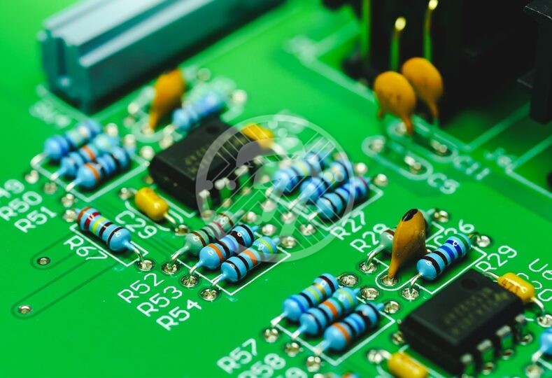
Solder Bridges becoming a major challenge during PCB assembly

The next generation Mantra is to provide uniqueness in the electronic solution raising the level of innovation in this modern world of electronics. The main innovation grounding the electronic manufacturing mechanism is the printed circuit boards. With this, it is important for the electronics manufacturer and OEM’s to update on the major challenges in pcb layout and assembly. Solder Bridges during PCB assembly are becoming a tough challenge for both the PCB manufacturers and the customers. This article is a brief guide for all the Original Equipment Manufacturer (OEM’s) to know the importance of solder mask during PCB assembly and pcb layout to prevent solder bridges. It also takes you to the root cause and preventive measures to avoid solder bridges during PCB assembly and avoid damage to the components and circuit board resulting into a PCB rework.
To come up with a perfect PCB prototype, The pcb layout and PCB assembly stage play a vital role in deriving a proper electronic manufacturing and design solution. Be it a PCB used in aerospace, defense, military, renewable energy, transportation, telecommunication or any other industries, the PCB manufacturers need a well defined PCB manufacturing process that uses quality raw materials and comes up with an exact pcb layout that prevents solder bridges or PCB rework with giving highly durable and effective solution in turn saving time and money for the electronic manufacturers.
To get insights into the things to be taken care of at the time of PCB assembly, all the electronic manufacturers should first understand the common major problems to be considered. Among all, solder bridges are the main blunder to be taken into consideration. With this, it is significant to understand the solder bridges at the prima facie.
Solder Bridges:
A solder bridge is an unwanted and unintended electric connection occurring between the conductors due to a small blob of solder. They are also known as “shorts” in PCB terminology. Detecting solder bridges are a difficult when there is involvement of fine pitch components. If it is kept unresolved, it can lend up causing a damage to the other components and the circuit board as well. The solder mask (ie) a thin layer of polymer applied to the copper traces on the printed circuit board to protect it from oxidation and avoid solder bridges forming between the solder pads. This solder mask is necessary for the mass production of the PCB but it is of less use in case of hand soldered PCB assemblies. For the circuit boards to be soldered automatically, Solder bath and Reflow techniques are high in trend. To avoid the solder bridges during the PCB assembly, it is first needed to decide a proper type solder mask to be used during the PCB assembly. This becomes a sensitive point of consideration while deriving a proper pcb layout and type of PCB for your project.
The electronics manufacturer should investigate thoroughly the merits and demerits of each type of solder mask and then decide whether to opt for Epoxy Liquid, Liquid Photoimageable Solder Mask (LPSM) or a Dry Film Photoimageable Solder Mask (DFSM). They can even take help of PCB manufactures to get a consultation and to go for a perfect type of PCB assembly with well defined techniques and flow of PCB production. For all the electronics manufacturers, though the prevention of the solder bridges can cause additional investment of time and money, but it can help you to derive a significant long term payback.
Causes of Solder Bridges:
The root cause of the solder bridges is the inappropriate pcb layout. Less than the idea package size of their components and also inadequate use of material melds has increased with the requirements of introducing more compact and faster technology. This is a big challenge for the OEM’s to go for a perfect and adequate layout of the printed circuit board. They usually end up compromising on the PCB layout to launch a new product in the market.
Other causes of solder bridges include the lack of solder resistance in-between the pads on the circuit board. The insufficient layer of polymer on the copper traces of a PCB usually known as a solder mask also acts an issue leading to solder bridges. When the device pitch is 0.5 mm or less, the inappropriate pad to gap ratio also becomes the cause of the solder bridges. The incorrect stencil specification can lead to excessive solder paste thus causing the solder bridges. The uneven distribution of the solder paste due to the inappropriate sealing between the PCB and the solder stencil, inappropriate stencil thickness, errors in the Surface Mount Component Placement or compared to the PCB-the solder screen has a poor registration, these are the common issues leading to solder bridges during the PCB assembly.
Remove Solder Bridge
To verify that the solder resist is applied between each lead and if it is not possible due to tight tolerances, then it accounts for a design change around that particular component. Also the recommended solder stencil of 0.127 mm thickness, stainless steel stencil with a laser cut works well for a device pitch of 0.5mm. These are the preventive measures to avoid solder bridges and to get a perfect PCB assembly solution. Checks out handy tips on PCB Solder mask.
TechnoTronix is one of the kingpin in delivering a well defined and proven pcb layout and PCB assembly service to the electronics manufacturers. Our main strength lies in the extensive experience and skilled team of experts to provide tailored electronic design and manufacturing solution. You can drop an email to sales@technotronix.us or give us a call at 714/630-9200 to solve your queries or to get a quote. To get more insights into the PCB assembly, layout and prototyping services, visit www.technotronix.us


