Basics To Drilling And How Precise Drilling Can Reduce The Cost Of PCB Fabrication?

By | Date posted: | Last updated: December 11, 2025
pcb-drilling-1

With the speeding up of innovations in high performance electronic devices and equipments, the growth of electronic industry has taken a step ahead in development across the globe. Electronic innovations are rolling out magic, be it automobile, military, aerospace, defense, marine, telecommunication and many other sectors. One of the bases and prime product used in the electronic gadgets is the High Density Interconnection (HDI) build up printed circuit boards. These PCB has an electrical conduction between the wrings on every layer which is controlled by internal layer vias. This is where the drilling plays a crucial role in pcb layout and manufacturing. This article is a guide to the basics of drilling holes on the circuit board. It highlights the current trends in drilling technologies. The blog also updates you with how drilling can help reduce the costs?

A few decades back, PCB drilling was done with a simple drill press. The drilling operator had to move the panel manually to adjust and correct x and y coordinate and tug the lever to drill which was a time consuming operation. With the technology advancement, becoming a constant affair in the electronic market, new drilling technologies are introduced which can now, suffice a PCB to have more than 10000 drilled holes of different size. Let’s dive more into the drilling operations in pcb layout and PCB fabrication.

PCB Drilling

When holes are drilled typically on a board base to thermally and electrically connect the board layers is known as drilling on a circuit board. These holes when connects the board layers is called vias. The main purpose of performing a drilling operation in the PCB fabrication process is to insert a through hole component lead or to connect the board layers for developing smooth circuitry on the PCB. This becomes a crucial part of the project from the very start that includes deciding on pcb layout, the materials to be used, method to fabricate the PCB and the type of vias needed to connect the board layers. Taking one wrong step can prove to be a costly affair as one tear or mar on the trace can make a show flop ending up with more use of the material and defect in the batch of production. Check out the guide to know more about Multilayer PCB Fabrication Process.

PCB Drilling machines and drilling technologies

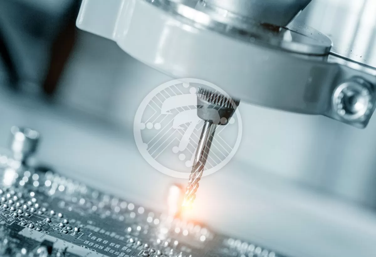
This drilling process is made easy with the innovations in technologies over the years. Now PCB drilling can be done with small diameter drill bits, automated drilling machine, CNC drilling machine and many other effective drilling machineries that can suit with the PCB manufacturing of multiple type of circuit boards.

Automated drilling machine can drill the holes in the circuit board by controlling the drilling operations with a computer. When many holes need to be drilled of different sizes and diameter, CNC machine is one of the effective solution saving time and cost of production.

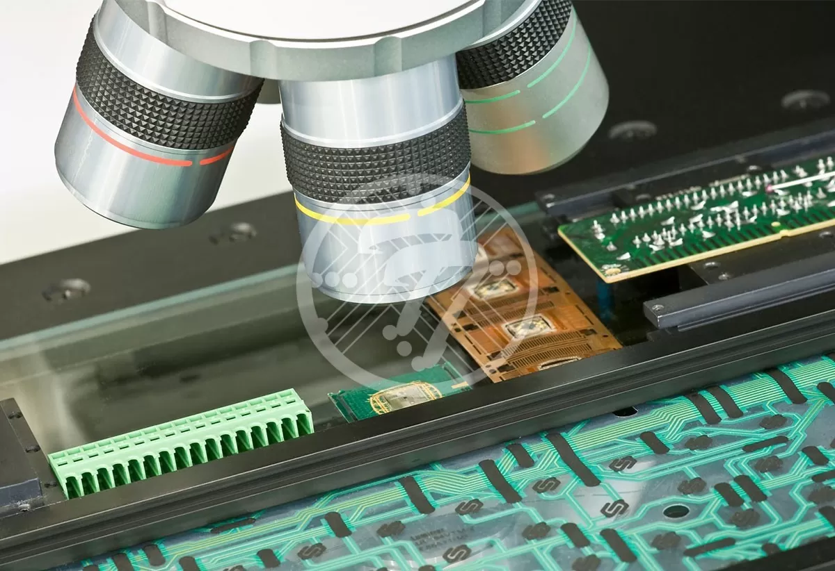
In case of drilling registration holes to make sure that further drilling performed on the center of the internal layer pads will be precise, an x-ray drill is used. This technology is used when via holes are linking copper layers together and holes are drilled on the leaded components.

In case of vias with very small diameter, using mechanical drill bits caused increasing of breakage on the circuit board in turn increasing the cost. So researchers have come up with a laser drilling technology to get a precise solution for drilling minute holes without breakage on the circuit board. When very small holes are drilled in, the board and connected with the board layers, they are termed as micro vias. One of the extensively used drilling technology in current times is CO2 laser drilling, which is used for drilling and processing internal layer via holes.

In case of holes to be drilled for connecting only some copper layers instead of passing through the whole circuit board, one can go for a controlled depth drilling or performing pre-drilling on the sheets individually before PCB lamination or laser drilling mechanism.

It is recommended to take the help of PCB drilling experts at the initial stage of the PCB project while deciding on the pcb layout and technique of production in PCB manufacturing.

How can precise drilling help reduce the cost?

The cost of drilling well be lower when the phase of drilling operation is performed at an optimum speed. In drilling the holes in the circuit board, every operation should go hand in hand. By drilling the holes faster, the speed should also be controlled to ensure the issues of tool breakage is not a problem. This controls the drill size to board thickness ratio. With this, by controlling the time consumed for pcb layout, cost can automatically be under control.

Thus, with the efforts to reduce cost, the research and development is also heading towards getting smooth conductivity between vias and have an effective component mounting with ensuring each drill has been successfully got registered and finished the tool path.

The tool room has well developed and upgraded technologies with a team of experts that adds value to our services in turn providing quick turnarounds and effective operations in PCB fabrication. Check out our PCB fabrication services. You can drop an email to [email protected] or give us a call at 714/630-9200 to solve your queries or to get a quote.

Magnitude Of Developments And importance Of Laminates In PCB Fabrication

By | Date posted: | Last updated: December 11, 2025
PCB Laminate

This present world entails the innovations in high performance electronic equipment that in turn demands for PCB laminates having highly developed properties with improved electrical attributes and better mechanical stability. The PCB laminate manufacturers are now heading to proffer a wide range of high performance laminates. These new versions of circuit board laminates have rich properties that curbs that of the conventional once like Epoxide based FR4 laminates were issues related to flame retardancy of laminates and electronic assembly temperatures are not a challenge anymore. This article is a detailed guide that pinpoints the basics to laminates in the PCB manufacturing process. A short drive to the varied types of laminates, properties of laminates with its importance and new development in laminate technology is what it has tried to highlight.

Well! Before going into brief about the importance of PCB laminates, let’s first have a short drive to the basics of circuit board laminates and more details on what are they? This article will lend you up to the exact understanding one should have at the time of deciding on the materials to be used in printed circuit board manufacturing and the type of laminates to opt for that is perfect for the specific project.

Types of PCB Laminates:

A stack of materials when laminated in the trace layers inside the board by applying pressure and heat for required time is called PCB lamination. This makes it a one piece product with lamination to the top and bottom pre-preg and then copper foil. In short, it consists of a typical process to laminate the non-conductive substrate with conductive tracks and pads that are etched from copper sheets that can help get a smooth circuitry connection with mechanical support to the printed circuit board. The basic materials used and processed in PCB fabrication include copper clad laminates, Pre-preg (Resin impregnated B-stage cloth), copper foil and laminates. These are manufactured by curing temperature and pressure layers of cloth or paper with thermoset resin that forms uniformly thick integral piece to get a final laminated base.

The use of fiber material or cloth, cloth to resin ration and the resin material determines the type of laminates. These laminates can be determined based on the requirement of the level to which it is free retardant, tensile strength, glass transition temperature, loss factor, shear strength, dielectric constant and expansion coefficient that reflects the thickness change with temperature.

The FR-4 has been the standard one that now being replaced by the many new technologies that give a more effective electric solution. These are composed of woven fiberglass with epoxy resin that have their application in switches, arc shield, relays and screw terminals. You can check out the effect of woven glass laminates on PCB. Considering the importance environmental safety, halogen free circuit board laminates is trending the upcoming innovation. Growth is marked in the Polyimide laminates that are rich in features with physical flexibility and high heat tolerance applied in High Temperature Fuel cells that has created increased demand in aerospace, military and electronic industry. One of the robust laminates used for outdoor environment application that has a great fighter to high heat conditions ceramic is proving to be an apt solution. No doubt it can prove expensive when high speed data transfer is required, but it has its applicability in solar energy projects. Thin printed circuit board laminates are used in high frequency applications, for instance the use of thinner substrates in millimeter wave or microwave applications.

Properties of laminates:

Properties of laminates that are trending the research and development in current times should also be brought to notice before selecting the PCB technology that is best for your electronics design and manufacturing project. The laminates having exact mechanical, thermal and electric properties should also have sufficient and tough chemical resistance, humidity resistance and fire retardation. Other properties to be taken care off are a resistance of foil, resistance to corrosion on the surface and edge, fine surface finish and thickness tolerance, flammability and water absorption.

Importance of laminates in PCB fabrication

Coming down to our main point of concern, there are vital traits about why we use laminates in PCB manufacturing? The importance of laminates in PCB fabrication that is in the mainstream includes to get an improved impedance control, low moisture absorption, better thermal management and consistent performance in dynamic thermal reactions. With new discoveries and constant innovations trading off in all the electronic assignments, high frequency laminates are becoming a core factor for the upward slope in growth of PCB technologies.

Technotronix is a skilled and experienced professional in providing apt pcb layout and PCB fabrication service. Our strong team of researchers and technical experts have made it possible to provide an effective lamination solution for your PCB project. Be it high frequency laminates, shrinking hole to hole pitch, exotic vias structures, multiple lamination cycle, lead free or halogen free solder assembly with strict environmental security considerations and high operating temperature are some of the highlights to our tough laminate technology implementation. You can drop an email to [email protected] or give us a call at 714/630-9200 to solve your queries or to get a quote.

Conformal Coatings Becoming A Core Driver To PCB Fabrication Done For Automotive Electronics

By | Date posted: | Last updated: December 11, 2025
Technotronix Blog

This advanced world of innovation has made it possible for the automotive electronics come up with fresh ideas and new technologies every other day.  The driver less car, EV’s, hybrid car, dual fuel vehicles and other recent buzz in automotive industry has raised the developments in miniaturization, multi feature application with tough and compact electronic solution. With this, security and safety are becoming a great sense of concern for the car manufacturers and other OEM’s. Selecting safe PCB that best suits the electronic application in the vehicle is also a difficult task for both the vehicle manufacturers and the PCB fabricator. The PCB needs proper coating to increase durability and its estimated life. Among all, the conformal coatings protect the PCB component from environmental stress.This article outlines the importance of conformal coatings and how it increases the PCB performance in the automotive electronics.

Commonplace for Automotive Coating:

Nowadays, the luxury features in a car are becoming a common requirement for the consumers. The standard features in a vehicle include rear facing cameras, automated parking system, lane departure warning system, driver assistance system and many more. While the high tech vehicle software for navigation, communication, networking, music and other technology are becoming commonplace.

More and more electronics are used in new vehicles that calls for attention to security and safety solution for electronics. The cars of current times have an inbuilt system for air bag control, automatic transmission, fuel injection system, power doors and windows, suspension control and engine control modules. This has made the researchers and investigators to focus not only on the vehicle software but also on the high quality tough hardware as well. This is now becoming a great challenge for the OEM’s and the car makers to decide a perfect PCB to be used in manufacturing that can provide a protective vehicle electronics in the next Gen innovations.

Importance of Circuit Board Conformal Coating:

The engineers have now come up with different solutions to protect the PCB for automotive applications. After considering various options like placing the circuit board in an enclosure or circuit board can be plotted with a resin, the best way to get safe PCB assembly and design is to use a conformal coating. For this, lets first dig into the meaning of conformal coatings.

The polymers applied in a thin layer of the circuit board to electrically insulate PCB components and protect it from the environmental stress are Conformal Coatings. These types of coatings are best for the compact PCB’s as they occupy less space. There are many ways to apply a conformal coating to the printed circuit board. Dispensing by a robot, spraying, flow coated or brushing are methods to apply such type of coat depending on the kind of production, be it on a massive, low or medium level production level. This safety coating can also improve PCB performance and increase the level of durability as it protects the circuit board from the humidity, thermal and mechanical stress, contaminants and corrosives that include fungi, salt, noxious gases and dirt.

Moreover, most of the lead-free printed circuit board assembly for automotive projects, notes ‘tin whiskers’ a common challenge that spurs the growth by thermal and mechanical stress leading to short circuits. The pace of this growth can be reduced by preventing short circuits and arcing through conformal coatings in the PCB. Adding more to the benefits of Circuit Board Conformal Coating, it improves the fatigue life of the solder joints with increased mechanical support.

The printed circuit boards are placed wherever they fit perfect for the car control system. From brake fluids to the gasoline fumes to the internal combustion engine, the PCB’s needs right type of coating without affecting the vehicle manufacturing process. PCB with conformal coatings are a main driver to secure electronic solution in the automotive realm.

These conformal coatings are available in a wide range depending on the type of PCB and its use. Urethane Acrylates, Silicones, Solvent based formulas and two part epoxies are the safe chemistries of coatings. While the light curable coatings also have their own advantages to provide a protective PCB solution for automotive electronics. Well, choosing correct coatings for PCB manufacturing needs proper consultation of PCB manufacturers and PCB expert. They can give a proper guide on selecting a protective coating for the PCB to be used in car and other automotive electronics. They perform qualification and environmental tests to simulate the conditions to which the particular coating will best suit for a particular application. These investigations include testing the temperature extremities, abrasion, moisture, vibration, chemicals, salt spray and other hazards.

Technotronix is a skilled and experienced professional in providing secured automotive electronics and PCB fabrication service. Our strong team of researchers and technical experts has made it possible to provide an effective lamination solution for your PCB project. Be it high frequency laminates, shrinking hole to hole pitch, exotic vias structures, multiple lamination cycle, lead free or halogen free solder assembly with strict environmental security considerations and high operating temperature are some of the highlights to our tough laminate technology implementation. You can drop an email to [email protected] or give us a call at 714/630-9200 to solve your queries or to get a quote.