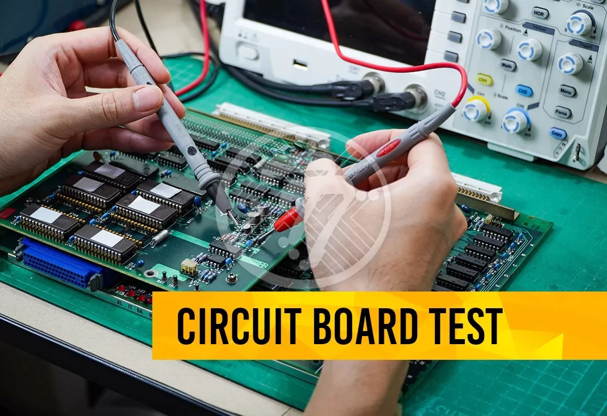
What makes flexible PCB board the best choice for satellite applications?

By | Date posted: | Last updated: December 11, 2025
Flexible PCB Board

When it comes to satellite applications, the use of flexible PCB boards is only growing! Not without reason! There are a large number of benefits that are pushing industry players towards the adoption of flexible PCBs. From reduced weight to increased reliability, there are a whole lot of advantages that flex PCB offer. Before we look at some of these advantages in detail, let us first understand how a satellite operates:

How does a satellite operate & what is its use case?

The satellite system has 3 main circuitries, namely:

  • Satellite
  • Receiver
  • Transmitter

While the communication between a satellite & transmitter is referred to as uplink, the one between the satellite & receiver is referred to as downlink.

The use cases of satellites include:

  • Disaster risk management
  • Weather Forecast
  • Remote Sensing
  • Geo-Positioning
  • Navigation
  • Telecommunication
  • Emergency Response Monitoring

Satellites, in turn, can be of 3 types, Fixed, Mobile & Broadcast, depending on the services they offer. A Fixed Satellite Service uses fixed receiving stations. These are primarily used in cable TV and internet stations. Mobile satellite services also deal with mobile systems for communication with fleet vehicles. Broadcast Satellite Service broadcasts TV & radio signals.

Given the functions that satellites perform, let us now look at the need for flex PCBs in satellite applications.

Advantages of using flexible PCB board in satellite applications

Reliability

Satellites represent mission critical operations and failure can come at an extremely high cost. It is imperative therefore that the PCB being used is extremely reliable. With flexible PCBs being able to withstand higher stress than rigid ones, they are suited for use in satellites that are subject to harsh environmental conditions. Additionally, Flex PCBs take away the use of connectors, which often cause interconnection failures. You are therefore assured of reliability when it comes to the use of flex PCBs in satellites.

Adaptability

The big advantage that flex PCBs offer is they are extremely adaptable, and land lends itself to shapes that ’t regular. Flex PCBs can fit into different surfaces that they are mounted on. However, this is not possible with rigid PCBs that cannot be used in complex shapes.

Their flexibility also comes in handy when you need extensible parts. With flexible circuits you can make use of expendable equipment without any fear of wear & tear.

Lightweight

With thinner copper layers as well as insulating layers, flex circuits are lightweight and can also adapt to tighter spaces with low bend radius.

While flexible circuits are made out of many materials, Kapton is particularly widely used because of its light weight. In addition, it is also known for its mechanical properties as well as vibration resistance.

While Flex PCBs are therefore well suited for use in satellites, it is imperative that PCB designers take the following conditions into account while designing PCBs for satellites:

Operating Temperature

It is important that the material chosen for PCBs to be deployed in satellites is suited for the harsh operating conditions. In fact, the material chosen should be able to survive in elevated temperatures of 120 degrees Celsius, or more.

Outgassing

When a PCB operates in a high-pressure environment, the gases trapped in the PCB are released. The gas released can condense on other sections and cause operational issues. It is therefore important to choose a material with good thermal resistance so that outgassing is controlled.

Orbital Collisions

With satellites, orbital collisions can be a reality. The PCBs should therefore be able to withstand such collisions. To ensure that, the flexing capacity of the PCBs should be high.

PCB standards for use in satellites

Because of these unique issues, there are specific standards when it comes to space applications. The common standards include:

AS9100

Created by the International Aerospace Quality Group, this standard is useful for creating products for the aerospace industry. AS9100D is the latest standard that the aerospace industry needs to adhere to.

The other standards that Aerospace as well as military-grade PCB assemblies need to adhere to include:

  • MIL-PRF-50884
  • MIL-PRF-31032
  • MIL-PRF-55110

To sum up

Rigid flex & fully flex PCBs offer several advantages over traditional PCBs. Their innovative design, reduced weight and more make them an ideal choice. It not only helps to minimize the size of the spacecraft but also improves reliability.

We have over 40 years of fabricating and assembling a wide variety of flexible aerospace PCB assemblies. With state-of-the-art equipment, we deliver the highest quality boards that you can rely on. Armed with an experienced flexible PCB board manufacturer team that can advise you on industry best practices, what you get when you join hands with us, isn’t just a vendor but a partner who is invested in your success. In case you have any questions, please feel free to contact us via email at [email protected].

Top signs that indicate that it is the time for a circuit board test!

By | Date posted: | Last updated: March 18, 2026
Circuit Board Test

The flawless working of a PCB is the key to the reliable working of any electronic equipment. It is therefore imperative that you be watchful of signs that indicate that your circuit board is faulty & that indicate that it is time for a circuit board test. Here are the aspects to look out for:

Common signs and causes of PCB failure:

Burnt Components

When the PCB needs to work under extreme temperature conditions, burnt components can be a reality. There are several factors that can result in burning of components, important among them being:

  • Area surrounding the component
  • Shape & size of the component

Overheating of components is a sign that all is not well with the PCB. Not paid due attention to, it can lead to operational issues.

Issues during manufacturing of PCB components

Issues in either the manufacturing of components or their improper placing can result in a number of issues. Some of the common issues faced include:

  • Improper soldering
  • Chemical leaks
  • Poor connectivity between layers
  • Loose components
  • Other human errors

An easy way to check for any issues with SMT components is to conduct a dye- and- pry test. It will go a long way in telling you about the issue & how the device is being impacted because of it.

Environmental Factors

In assembling electronic components, it is extremely important that environmental conditions are controlled. For example, humidity in the room can lead to a wide variety of issues. Similarly dust & heat can impact the PCB, as can issues such as an accidental fall. Some of the other causes that can lead to malfunctioning of PCBs include accidental submersion in water or exposure to lightening, for example.

Also, overtime dirt can accumulate in the PCB & cause it to malfunction as also reduce its lifespan.

Age of components

As components age, circuit boards can eventually fail. In fact as components reach end of life, malfunctioning can increase many fold. Component replacement at this stage may therefore become a reality.

Armed with this information about potential causes of PCB failure, the importance of printed circuit board testing cannot be overstated. Testing can reveal issues that can be addressed through rework & repair.

If you already suspect that your circuit board may be faulty on account of the above reasons, what then are some of the recourses available to you?

What to do in case of a suspected faulty circuit board?

1. If the board’s electronic components are in place, the first thing to do is to test the board with its power on.

2. In case electrical components have not been installed, the power needs to be shut and the connection wires cut, before the board is inspected.

3. It is important to check the circuit board for any visible signs of damage. Signs can include components that are crushed, wires that are cracked, any burn marks or scratches and more. Scratches can damage connections while misplaced solders can disrupt connections or even cause a short circuit. In case such signs are visible there is no need to continue the testing. Instead the damaged parts need to be immediately replaced.

4. Switching the circuit board on & checking for the voltage of all connections with an oscilloscope is an important step. Voltage probes need to be applied to the end of each connection so as to be able to identify the issue.

5. In case connections aren’t conducting the specified voltage, what is indicated is a bad connection.

To sum up

Over a period of time, PCBs can undergo damages that can impact their functionality and therefore the functionality of your electronic device. Timely testing can ensure that the board is repaired or reworked. Of course, understanding the exact issue is the vital first step to be able to make the necessary repair. Knowing the signs of PCB failure can therefore go a long way in ensuring that you take timely action & that the functioning of your equipment isn’t compromised. Needless to mention, that in mission critical operations timely testing & necessary action can be life saving.

TechnoTronix is an ISO 9001:2015 certified company who delivers one-stop PCB manufacturing services with specialized support, reliable testing, and multi-functional features. Our main strength lies in the extensive experience and skilled team of experts to provide error less and lead-free PCB manufacturing solution. You can drop an email to [email protected] or give us a call at 714/630-9200 to solve your queries or to get a quote.

What are the design considerations and guidelines of round circuit boards?

By | Date posted: | Last updated: December 11, 2025
Round Circuit Boards

Today, PCBs are available in a wide range of shapes, even though square and rectangular PCBs remain the most common. With the ever-developing electronics industry, the one shape that is gaining prominence is round PCBs.

As the name implies, a round circuit boards is a PCB that comes in a circular shape. It is often used in consumer electronics, wearable devices and more.

The advantage with round PCBs is that it offers increased board space. Fabrication of round PCBs however requires a lot of care since it is a complex process. In fact, the routing process of a round PCB requires a lot of time. All of this also has a repercussion in terms of the overall costs of round PCBs.

Types of Round PCB

Round PCBs, in turn, are of different types. These include:

  • Single-sided PCBs
  • Double-sided PCBs
  • Multilayer PCBs

A single sided round PCB comes with one conductive copper layer. This type of PCB is extensively used in low-density designs. Such a PCB has components on one side of the board while there is a conductor pattern on the other side. Such PCBs use either through-hole or surface mount technology.

Double-sided round PCBs have conductive layers on two sides of the board. They are extensively used when it comes to applications such as wearable devices, lighting systems & more.

A multilayered round PCB has more than two conductive layers. Even though they are the hardest to fabricate, they offer multiple advantages including:

  • They lend themselves to higher density.
  • They offer increased board space.

Round PCB Design

It is a given that round circuit boards are more complex when it comes to the design bit. Thankfully though there are few tools available that aid the design of a round PCB. There are several design rules, however, that need to be followed when it comes to round circuit boards. For example, the perimeter of such boards can only be shaped with a straight-line segment. Also, in arranging the lines of the perimeter, a circle needs to be placed on the silkscreen layer. Let us look at some more PCB layout and design rules in detail:

Round Circuit Board Design Rules

  • First & foremost, when using the CAD tool, it is important to draw the shape in the CAD tool.
  • Of course, if the round circuit board is being designed for a high-speed appliance, your choice by default will have to be a multilayered printed circuit board.
  • The power and ground planes need to be defined in separate layers. A polygon editor can go a long way to define the shape of ground or power planes.
  • Some software also offers the option of customizing the power & ground planes.
  • What also needs to be kept in mind is that round circuit boards need panelization schemes for their design.
  • To panelize a round PCB, break routing is widely used. It is imperative that a 10 mm (about 0.39 in) clearance is kept between the round circuit boards. With a larger routing tool, however, the clearance can be increased.
  • As far as the mounting technology goes, both SMT (Surface Mount Technology) as well as THT (Through Hole Technology) can be used to place components, although SMT is better suited.

To sum up

Overall with Round PCBs, designers have a lot of flexibility. The added advantage also is that there is the possibility to incorporate more features as you go along. Also, with the help of CAD tools the designer can add pad shapes in the circuit board.

While such boards are complex to design, the use of the right software can aid the designing process. Following design rules & best practices can also go a long way in making eth process seamless. It is also imperative that you deal with a professional electronics contract manufacturer who is involved in the PCB design phase itself. That way, the manufacturer can assist you with the best practices & point out any design flaws early, so that you do not have to contend with any costly issues at the fabrication stage. Needless to mention that design issues once the board is manufactured can sometimes even lead to irreparable damage to a company’s reputation.

At Technotronix, we are fully equipped to handle your PCB manufacturing requirements. With over four decades of experience in delivering high-quality, on-time, competitive price products, you can rely on us for your PCB requirements. In case you have any questions, please feel free to contact us via email at [email protected] or call us at 714/630-9200

How to fix common PCB Gerber file issues?

By | Date posted: | Last updated: March 18, 2026
PCB Gerber File

With electronic technology making its way to different fields, the use of PCBs has become ubiquitous. PCB designers & manufacturers are therefore increasingly working towards developing PCBs that are robust & more efficient. This is extremely critical especially when PCBs are being deployed in mission-critical operations where any mistakes can turn out to be extremely costly. One way to do this is to ensure that the Gerber files and the digital blueprints of the PCB are robust. Any errors in the Gerber files can prove to be fatal as they can lead to PCB failure.

Ensuring that Gerber files are therefore complete & accurate is key. Let us look at how to fix PCB gerber file problems.

Here are some of the most common ways to fix common PCB Gerber file issues:

Empty Gerber Files: It may sound incredulous, however, there have been enough & more instances where a Gerber file is an empty or a “zero-byte” file. This can happen on account of many reasons, the most common one being that the data is accidentally deleted. It is therefore imperative that each Gerber File be properly checked before it is sent onwards.

Incomplete Files: If enough attention isn’t paid to the PCB Gerber files, you could have instances where the Gerber file is incomplete. Missing information can prove to be dangerous as it may lead to a board that does not match up to the desired levels.

Improper Labeling: If the labeling of the Gerber files isn’t in line with the established protocols, it has the scope of leading to a wide variety of errors.

Too Many Aperture Lists: It is important that the Gerber File has a single aperture list with all the details. Multiple aperture lists are a source of confusion. It is also important that the format of the aperture list is the same as that of the Gerber Files.

Composite Layer Design Errors: In case composite layers are generated while generating individual layer design specifications, the images need to be combined so that one Gerber file is created for each layer.

Missing Board Outline: Sometimes when PCB Gerber files are generated, the board outline is not produced by default. It is important that the actual bounds of the board edge be described.

Missing Drill files – A drill file is required to create any through-hole footprints that might be present in the design. For software packages where a separate option is required for generating drill files, it is important that it is not missed.

Issues with other design files – It is always good to crosscheck that any revisions that have been made to your design are reflected in the Gerber files, Bill of Materials as well as the Centroid File so that there is no scope of any error.

Vectorized Pads: In some cases, rather than generating the pad as one solid object in the Gerber files, the software may output a cluster of small vectors that together form the pad. It is important therefore that the software is set at generating “ Flash Pads” as opposed to “Vector Pads”.

To sum up

While the good news is that it is easy to avoid Gerber File errors, the bad news is that any errors made can lead to far-fetched consequences; consequences that are expensive, time consuming and that can cost you your company reputation. As they say, it is better to be safe than sorry. It is important therefore that any sources of potential errors in Gerber Files are checked & fully eliminated. Some simple ways to ensure that you avoid Gerber File errors include:

  • Making use of a Gerber file viewer
  • Printing a simple board. This will allow you to see that the specifications are correct & that there are no errors or omissions.
  • Making use of high-definition CAD software
  • Importantly, making use of Quality Control practices throughout the design process.
  • Choosing your PCB partner with care. The right partner will ensure that a rigorous quality assurance process is undertaken. This will include checking the PCB Gerber file thoroughly so that there are no costly errors at a later stage & that the PCB that is manufactured is to the specifications & adhered to stringent quality parameters.

Technotronix is one of the leading providers of PCB manufacturing services to all the dominant industries. With over four decades of experience in delivering high quality, on-time, competitive products, you can rely on us for your PCB requirements. Also, you can drop an email to [email protected] or give us a call on 714/630-9200 to solve your queries or to get a quote.