What are the telecom PCB design considerations?


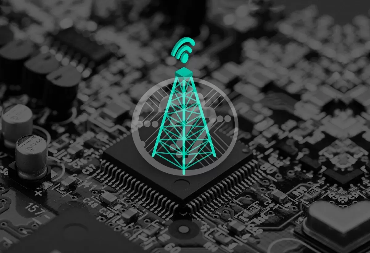
When it comes to designing PCBs for the telecom industry, there are a number of things to consider. Right from the PCB materials to the kind of testing required, there are factors unique to the industry; not to mention the fact that there are generally tough deadlines & budgets to work with.
Here are some of the PCB design considerations to take into account when designing for the telecom industry.
Telecom PCB Design Considerations
The specs
To begin with, it is extremely important to understand what is the size of the product, how the final product works, who are its target users, what are the features desired, and more. Additionally, it is important to think through how the device is being powered. Once you have thought through all these aspects you can rest assured that there will not be costly errors at a later date.
Software or Hardware?
It is important to determine whether you can add hardware components or software code to complete some functions. Each of them comes with its own set of advantages & disadvantages:
Hardware Advantages:
- Fewer security risks.
- Needs analog signals.
- Debugging is easy.
- Less chances of failure.
Software Advantages:
- Easy to update.
- No requirements of costly materials.
- Troubleshooting is easy.
The Microcontroller
Simply put, the microcontroller can be likened to the brain of the product. Therefore, it is crucial to choose the microcontroller wisely. Some of the factors to consider include:
- What are the programming options – In making the choice of the microcontroller, you can go with one that has internal memory or one that can interact with external devices. Similarly, you can go with one that has a one-time programmable option or reprogrammable.
- Whether or not the controller needs built in peripherals.
- What are the internal RAM requirements and can an external RAM be used for expansion.
- What are the technical considerations to get the microcontroller running.
Once you have an idea of the components required, the next step is to work on the schematics. You need to have the details such as the names, ratings, pins component values, and more.
It is imperative that you ensure that the bare board has enough space so that all the components can fit in.
Do not miss the fact that there has to be enough soldering mask between every pin. If this step isn’t done correctly, defects will soon surface.
PCB Component Placing and Routing
You need to make sure that component placement is done correctly so that the PCB can function effectively. Component placement also has a strong impact on thermal management as well as electrical noise, so it needs to be done with care. As a thumb rule, Components should be arranged in the following order:
- Connectors.
- Power circuits.
- Precision and sensitive circuits.
- Critical circuitry components.
Some of the other guidelines to follow, include:
- Place similar components facing the same direction. This will help reduce errors in soldering.
- When plated through-hole components are placed on the solder side, it is important to see that components aren’t placed directly opposite.
Quality Checks
This is a very important step once the PCB is completed. There are a number of tools such as a Design Rule Checker that can come in handy to spot any errors in design. Additionally, an Electrical Rule Checker is important to see that all specifications have been adhered to.
To sum up
It is imperative to follow six crucial steps when it comes to PCB designing:
- Conceptualization of the board.
- Draw the circuit schematic. When creating the schematic, it is also important to create a detailed bill of materials (BOM) that contains information on all the components.
- Define the mechanical constraints of the board.
- Ensure proper component placement.
- Ensure good routing that improves signal and power integrity.
- Run quality and manufacturing checks to ensure all requirements have been met. In case the design does not pass all the checks, you need to revisit the previous steps and make necessary changes.
At Technotronix, we have over 4 decades of industry experience. Importantly, we have dealt with a wide range of telecom providers. We are therefore well-poised to understand the various issues than plague the industry and how robust testing can help overcome these issues. To know more, please explore our PCB manufacturing services for Telecommunication Industry!