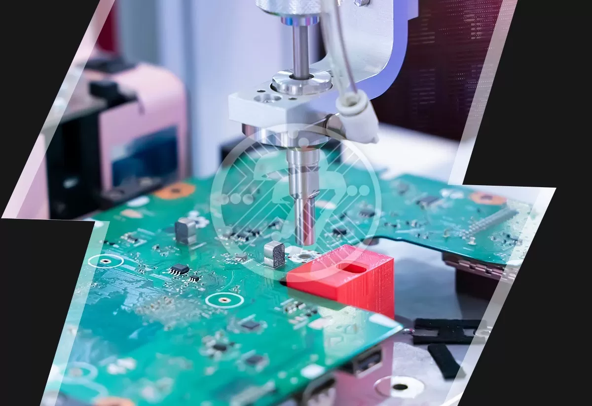
PCB Mouse Bites vs V-Grooves: What is the difference?


Before we look at the difference between PCB Mouse Bites & V-Grooves, it will be worthwhile to begin with looking at what exactly is PCB panelization and what are the various factors to consider in choosing the right technique from amongst the several available.
What is PCB Panelization?
Essentially PCB Panelization allows you to connect smaller circuit boards into a large array. The vendor performing panelization can equally easily depanelize the array. In fact, depanelization is known to increase throughput of PCB.
Factors to Consider for PCB Panelization
The choice of the panelization method depends on a wide variety of factors. Some of these include:
- Design – Aspects such as clearance between the board’s edge and its components, the presence of edge-hanging components can impact the choice of panelization
- Components- If the board has sensitive connectors and components, the choice of panelization techniques will be impacted.
- Materials – The type of PCB material used also determines the panelization technique. For example, some materials are prone to splintering. Similarly, if the boards are very thick you could face issues.
- Shape – The shape of the printed circuit board also impacts panelization.
PCB Panelization Methods
The broad methods of PCB Panelization include:
- V-Groove Panelization
- Tab Routing Panelization
- Performated Tab Routing or what is known as Mouse Bites
Let us look at PCB Mouse Bites versus V-Groove in some detail:
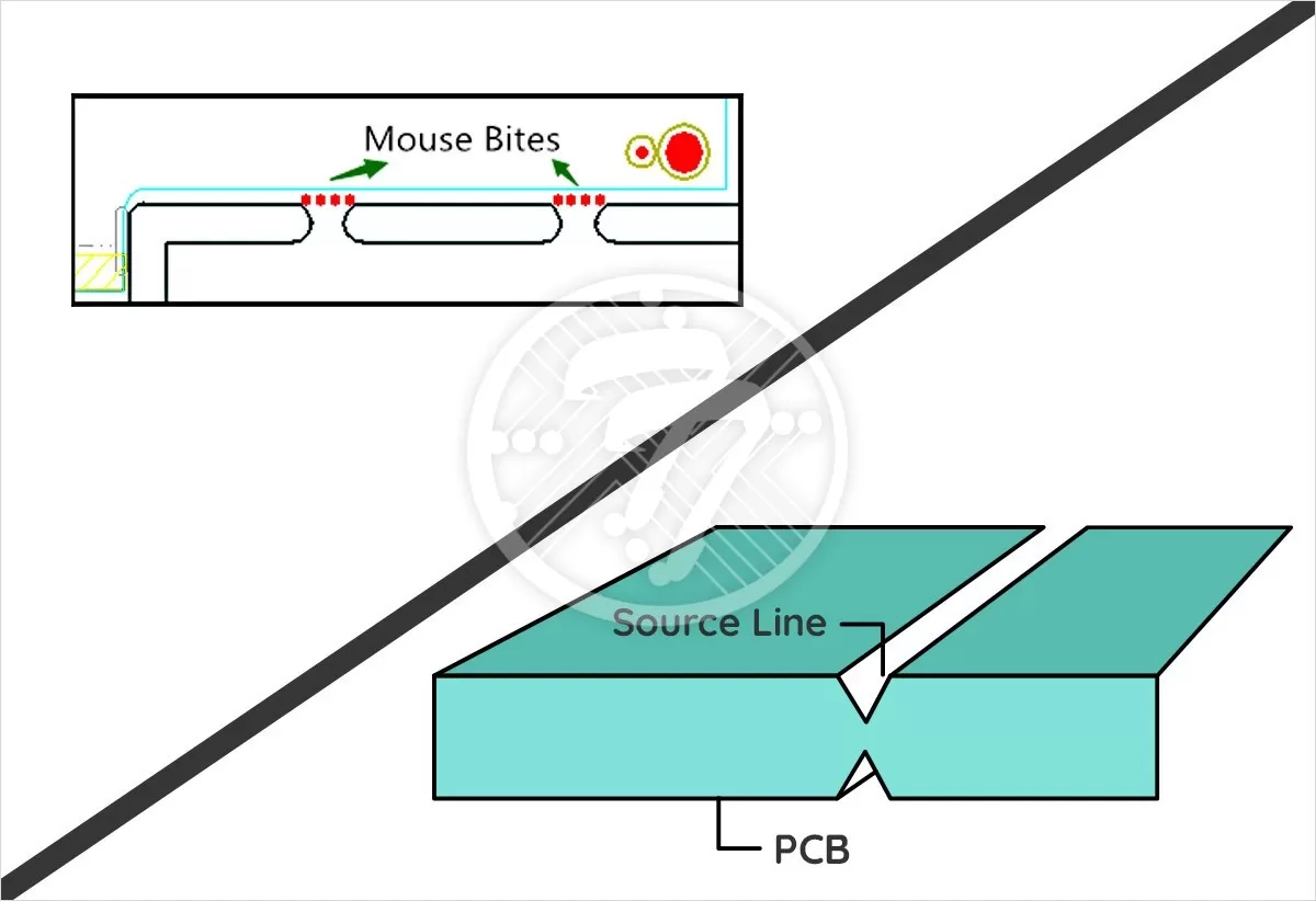
What is perforated tab routing or mouse bites?
This technique involves drilling small, perforated holes in tabs. It is in their similarity to mouse bites that this technique gets its name. The manufacturer pre-cuts the boards on the array and holds them in place with the perforated tabs.
This method works well where:
- The components aren’t too heavy
- It supports edge-hanging component designs which is a source of significant advantage.
The advantages of Perforated tab routing Or Mouse Bites include:
- They offer a good grip when mounted
- They work well if you want to use hand separation as a technique of separation.
With perforated tab routing, the areas of concern, however, remain as below:
- It leaves material on edges. It therefore necessitates sanding. In turn, this not only involves a cost but also consumes time.
- For holes more than 0.6 inches, a placeholder or knockout might be needed
- There is a chance of these popping out earlier than needed.
V-Grooves
Also known as V-scoring, v-groove panelization involves separating individual boards housing V-shaped grooves. With this method, the manufacturer can remove 1/3 of the thickness of the board from the top and the bottom. They need to be cut with the help of a machine typically at an angle of 30 or 45 degrees. This method does not lend itself to hand separation as it can put stress on the board as well as its surrounding components.
In this method, the panelization has to have a 0.05 inch clearance from the components to the groove’s center.
V-Groove panelization works well for square and rectangular shaped board. You, however, cannot use it to cut straight lines through the array.
Essentially, this method works well where:
- There are no overhanging components
- There are no round corners
- Where there is a sufficient distance between the component limit and edge of the PCB.
The other advantages of V-Groove include:
- It is more cost-efficient than mouse bites
- V-scores are easier to make
- They offer greater strength
The concerns with depanelizing V-scored PCBs include:
- It needs a lot of force to break apart and hence requires dexterity to see that components are not harmed during the process
- In case the copper traces are too close to the score, it can result in splitting.
To Sum Up:
PCB panelization has emerged as an important step when it comes to PCB manufacturing and assembly. By knowing the benefits and constraints of each of the methods outlined above, you can ensure that you do not make any costly mistakes. Also, by knowing the strengths and weaknesses of each technique, redesigns and delays can be avoided, significantly impacting your go-to-market and giving you the much-needed competitive edge.
Technotronix is one of the leading PCB manufacturers based in the USA. We have over 4 decades of experience in providing innovative PCB manufacturing services using modern technologies and the latest machinery. We are adhering to strict high-quality standards and compliant with the RoHS quality management system.
For Any Kind of PCB Manufacturing Service, Get a quick quote!