The effects of ESD (Electrostatic discharge) on PCBs


What is ESD?
Electrostatic Discharge or ESD as it is commonly called, occurs when two objects with different charges come close, so that the dielectric between them is broken. The common form of ESD that all of us are familiar with is lightning. Ever so often we could feel little sparks from a wool blanket, for example, which is once again a result of ESD.
How does ESD affect PCB?
When a PCB comes close to any object that has an opposite charge, it is subject to ESD. If the two come in contact, voltage is discharged and a massive voltage spike is created. Once the spike dissipates, electromagnetic fields are generated. It is therefore important to minimize the effect of the discharge. This is typically referred to as an PCB ESD Protection.
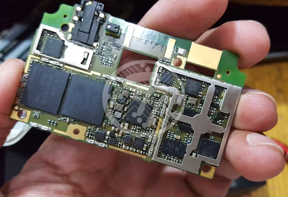
With modern chipsets having little tolerance for high voltage, an ESD event can as much as totally ruin the IC. The impact of ESD needs to therefore be factored in the design process of the PCB, as later it could lead to a host of redesigning to fix issues.
ESD can exist in many forms. While it typically requires several thousand volts for ESD to be felt by a person, even a small discharge can ruin semiconductors if the part is in the path of the ESD.
In turn this damage can be latent or catastrophic.
Catastrophic Damage:
This refers to the permanent damage to the device’s circuitry and can be detected using a performance test.
Latent damage:
This is said to occur when a device is partly degraded on account of being exposed to ESD yet continues to run even though its lifetime behavior is likely to be affected making the device unreliable.
Costly Effects Of ESD
While a catastrophic failure can be detected at an early manufacturing stage, it may not turn out to be as costly as a latent damage since it isn’t normally detected easily. As the product passes the regular inspection, latent failures can prove to be extremely costly besides impacting the company’s reputation.
What causes ESD?
ESD can be caused by a number of seemingly ordinary activities. A simple activity such as plugging in a cable can lead to a discharge. It is therefore important to protect your PCB from external connections as plugging in or pulling out a cable can expose the devise to the risk of ESD. There are, therefore, a number of precautions that can be taken to protect your PCB from the risk of ESD. Common precautions include:
- Using a copper land or pad to attach connectors
- Keep the pad separate from the PCB ground
- Use a Transient Voltage Suppressor to protect the board
It is also prudent to establish and identify an ESD Protected Area, which is a clearly demarcated space within which all surfaces, objects, people and ESD Sensitive Devices (ESDs) are kept at the same potential. Typically all surfaces are linked to the ground. The area also needs to be identified with a clear signage and should allow access to only trained personnel. Periodic checks of installed products are mandatory within the area while all non-essential insulators need to be removed. It is also important to identify ESD Sensitive items as also to provide adequate ESD Control training to the staff to ensure that ESD control procedures are followed. The staff needs to be aware of the threat of ESD as also the ways and means of controlling static electricity.
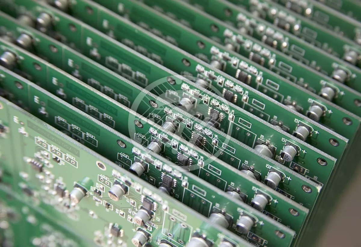
PCB Layout to prevent Electrostatic Discharge
Apart from this, a whole lot of PCB Layout practices can go a long way in protecting PCB. These include:
Remove circuit loops:
Loops can lead to unwanted current. This in turn affects performance as unwanted current spikes can enter any loop. Due care therefore needs to be taken to ensure there are no loops.
Utilize ground plane layers in the printed circuit board:
Using a ground plane within a circuit board can go a long way in helping to reduce loops and therefore unwanted current.
Reduce line lengths:
Reducing line length in effect reduces the radiated energy received and therefore reducing the spikes from electrostatic discharges.
Reduce parasitic inductance:
Protection circuits can only work effectively if parasitic inductance levels are low. In turn parasitic inductance can be reduced by keeping the line lengths short.
Avoid running sensitive tracks near the extremity of the PCB:
The extremities of the board are more likely to pick up static discharge. It is therefore prudent to keep sensitive lines away from the extremities.
With electronic circuitry becoming increasingly smaller, the sensitivity to ESD is on the rise. What therefore also increases is the need for proper ESD protection.
Technotronix offers Electronics Manufacturing Service with combining state-of-the-art technology and advanced engineering to deliver unparalleled quality and service. Our prolonged goal is to serve our customers with electronic telecom solutions for development in telecommunication industry and to create advanced IT applications for our customers globally. To acquaint with Technotronix, reach us at sales@technotronix.us to get more information about PCB Manufacturing services for electrical telecom applications or prototypes!