How UV Lasers helps in HDI pcb layout and Guidelines to design HDI PCBs

By | Date posted: | Last updated: December 11, 2025
hdi-pcb

With advances in UV lasers, the one industry that is definitely benefitting is that of pcb layout. UV Lasers allow for PCBs with shrinking vias, which in turn leads to a number of advantages but not limited to manufacturing dense PCBs at lower costs.

While with CO2 lasers, the micro vias had diameters of 60-80 µm, with UV lasers the same figure can be brought down to 15 µm. Additionally these can be drilled at high speed. In turn this leads to quick production. Also, with less power required to drill this vias, there is less generation of heat. This is especially advantageous where boards are mounted on paper. UV Lasers transfer minimum heat to the board and ensure that the board isn’t impacted.

The other advantage of small vias drilled with lasers is that vias with narrow diameters leads to production of smaller boards. What it means is that Making boards for Internet of Things, for example, where space is a constraint, becomes far easier. Small vias also enable use of other technologies such as New Ball Grid Array or Via-On- Pads which do not work well with traditional vias. Also smaller boards will typically mean lower cost of fabrication.

Another distinct advantage of small vias is that they radiate less EMI. Reduction in the size of the via means reduced impedance which in turn means less voltage drop.

The fact that these UV lasers also offer a distinct cost advantage also works strongly in their favour. Also being able to use these lasers for all cuts and holes allows the manufacturer to save money when it comes to fabrication. In fact the accuracy of UV lasers for cuts and channels also makes a strong case for their use.

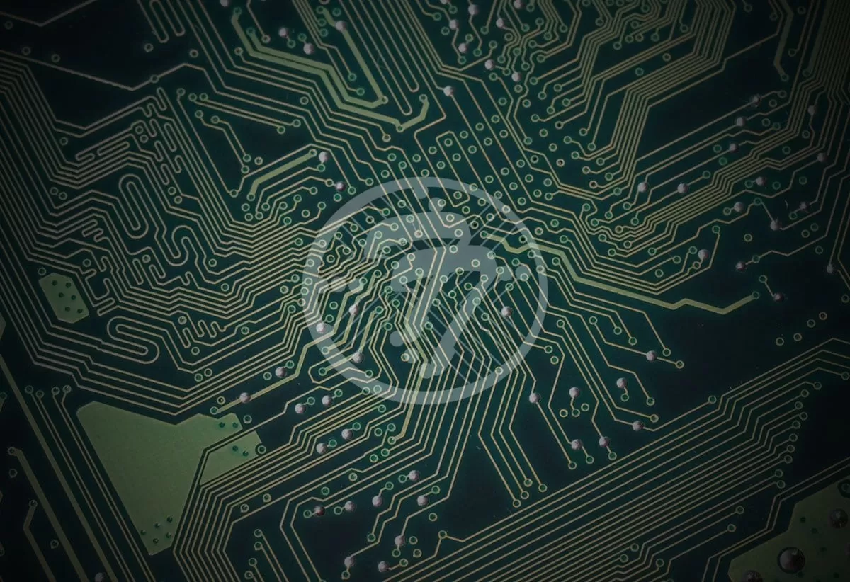
While UVs clearly offer a number of advantages in HDI PCB layout, it is however important to keep in mind that Making of HDI PCBs needs to follow some basic tenets which can then add to the PCBs performance. Compared to ordinary PCBs, the HDI PCBs obtain their interconnections through blind and buried holes. Additionally, small spacing is used in PCB Layout to fully utilize the space. To be able to do so, though, it is imperative that the process parameters in the HDI PCB manufacturing process are understood.

Here is a quick overview of the Manufacturing Process and some aspects to be mindful for HDI PCB Design:
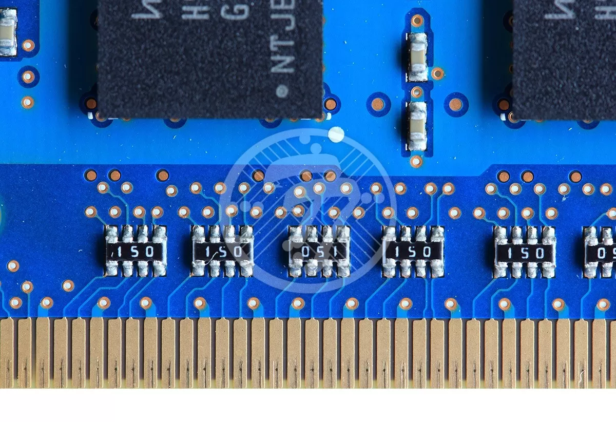
Aperture

One of the things to consider in hole design is the aperture ratio. In case of mechanical drilling through hole aperture should be more than 0.15mm and board thickness-to-aperture ratio more than 8:1. For laser drilling, however, the aperture of laser hole should be in the range of 3 to 6mil and the plating filling hole depth-to-aperture ratio at 1:1. Also the process of plating makes it difficult for the chemical solution to reach the drilling holes. With the increase in voltage, defects can spring it. It is important for PCB designers to know of these aspects to ensure there are minima issues faced during fabrication.

Stack

There are different categories of HDI PCB layer stack-up basis the order of layers with blind holes. Typical categories include:

  • 1-HDI (with buried holes)
  • Non-stacked 2-HDI (with buried holes)
  • Stacked but non resin filled 2-HDI
  • Stacked and resin filled 2-HDI

Process Flow

The sequence of drilling holes in case of HDI is crucial. For example in a 4 layer HDI, it is important to know that the sequence to follow is the mechanical drilling buried holes of 2-3 layer, followed by the mechanical through hole of 1-4 layer, and then 1-2 blind hole and 4-3 blind hole. If this sequence isn’t followed, the design can get extremely difficult to fabricate. In turn this leads to an increase in cost of production.

Layout

It is important to ensure that the component layout is correct which in turn lends itself to solderability as well as to maintainability. Some of the other aspects that need to be considered in terms of layout include:

  • Layout of the same module ideally should be on the same side
  • High power signals should not be close to other signals

Track

The other aspect to take into account includes areas such as uniformity of track and spacing. If the spacing isn’t adequate there is the risk of a short circuit. Similarly if the line width isn’t adequate, it could lead to an open circuit. Other aspects of the track that need to be borne in mind include:

  • Reducing cross talk between inner layer signals
  • Mono block pavements need to be avoided
  • Bind holes without physical connection interference should not be added to the track area

A fair idea about the parameters of HDI pcb layout will go a long way in helping designers in Making HDI PCBs that significantly improve performance.

At Technotronix, we are fully equipped to handle your PCB manufacturing requirements. With over 4 decades of experience in PCB manufacturing as well as assembling PCBs with differing levels of complexities, we follow industry best practices to ensure we deliver cutting-edge products. Our team of experts and state-of-the-art equipment ensures that all our PCBs meet the industry standards of quality and testing. It is our vast portfolio of satisfied clients that stand as the biggest testimony to our success. In case if you have any questions, please feel free to contact us via email at [email protected]

Does Biodegradable PCB can really reduce E-Waste Problem?

By | Date posted: | Last updated: December 11, 2025
biodegradable-pcb

PCBs are an integral component of every electronic gadget. With the increased use of electronic gadgets in various aspects of our life and also on account of their reduced life span, the one thing that is on an increase is the amount of electronic waste. With new industries such as Internet of Things and advanced driver assistance in cars burgeoning, the growth is only likely to be accelerated.

Why PCB waste is a real problem?

While PCBs are designed to last for many years, the fact is that gadgets in which these PCBs find pride of place, are being replaced at alarming frequency. A key issue that therefore arises is that of decomposition, leading to a host of environmental issues. With a high percentage of the discarded electronics going to landfills especially in the developed countries, they release toxic substances into the environment such as:

  • Mercury – That can cause kidney and brain damage.
  • Cadmium – That is known to cause cancer.
  • Lead – It is known to leads to brain damage
  • Brominated Flame Retardants (BFRs) – These are known to affect hormonal functions in women.
  • Beryllium – Is known to cause cancer

Even if the board is recycled instead of being thrown in a landfill, the recycling process is hazardous and can lead to health hazards. The added problem is that with our devices getting smaller and lighter, taking them apart to salvage recyclable components, is a huge exercise. All the glues, adhesives used need to be removed manually before any recyclable material can be withdrawn. The process therefore is extremely labour intensive. Typically what this means is that PCB boards are shipped to less developed countries where labour costs are lower. The answer to both these problems- electronics landing up in landfills or the issue of them being recycled- clearly is biodegradable PCBs which can go a long way in reducing e-waste. TechnoTronix is the leading name in providing renewable energy PCB prototype.

Replacing current, toxic materials with transient metals such as tungsten or zinc is a big step forward in this direction. A group of scientists at the University of Illinois Urbana-campaign Frederick Seitz Materials Research Laboratory have set out to create a fully functional PCB that disintegrates when exposed to water. The PCB is made out of the following:

  • Commercial Off-the-Shelf Components
  • Magnesium Paste
  • Tungsten paste
  • Sodium Carboxymethylcellulose (Na-CMC) Substrates
  • Polyethylene Oxide (PEO) Bonding Layer

In fact, completely bio degradable PCBs have been developed using bio-composites made from natural cellulose fibers extracted from banana stems and wheat gluten. The bio-composites are free of chemicals. These biodegradable transient PCBs have performance similar to conventional PCBs. Partially bio degradable PCBs have also been developed using chicken feathers and e glass fibers.

Biopolymers such as carbohydrates and proteins are bio-degradable but they need natural resources such as land and water which are becoming scarce. Renewable and sustainable biopolymers can also be obtained from agricultural wastes such as banana fibers, which are extracted from the stem of the plant. These agricultural co products can be used to develop completely biodegradable composites.

Are Environmentally friendly Printed circuit boards reliable?

Often times the words environment friendly conjures up images of a product that is fragile, which is not a property we would want to associate PCBs with. Some of the fears that we associate green PCB boards include:

  • Mechanical Properties- The fact that the environment friendly boards are made of banana fibers makes us assume that the boards could be as weak as a leaf. The fact however is that researchers are combining substrate materials to create boards that are comparable in strength to conventional boards.
  • Thermal Properties- PCBs need to perform highly on thermal performance and not catch fire easily. Biomaterials are known to have low temperature thresholds so in some sense this fear is well founded. However, low temperature solders help to circumvent this issue.
  • Dielectric constants- This is one area where bio degradable boards perform at the same level as traditional boards. The dielectric constants achieved with these boards are well within the required range.
  • Performance in extreme conditions- No deviation in output has been observed in case of the bio-composite PCB on exposure to high humidity or temperature.
  • Heat dissipation- Bio-composites are able to dissipate a significant amount of heat which is a desirable property for a PCB.

As the use of electronics becomes more widespread E-waste will continue to grow to alarming proportions. The good news however is that as research into environmentally friendly options further progresses, green boards will be a commercial reality, thereby reducing e wastes and the problem of electronics recycling. While we are contending with the e-wastes of the past as well as current electronic devices, it is time for us to look towards the future and ensure the widespread use of biodegradable PCBs.

With having a combined extensive year of experience in PCB fabrication, PCB prototyping, PCB assembling and PCB rework, TechnoTronix has created a strong customer base for varied industries to shape up new trends for PCB manufacturing across the globe. Drop an email to [email protected] to get proper consultation or share your requirements to get a perfect PCB with a cost-effective strategy, or give a call 714/630-9200!

Challenges faced by PCB Manufacturer in building of lead free SMT Assembly

By | Date posted: | Last updated: December 11, 2025
SMT Assembly

SMT Assemblies are getting more and more complex. While SMT Assembly makers strive for 100% yield, the fact is that achieving it is extremely difficult. While a majority of electronics today utilize SMT Components however the reduced component sizes make putting them onto PCBs extremely difficult.

There are a number of other defects that SMT Assembly has to overcome, primary among them include:

Poor Solder Paste Release
Solder Paste Release, in turn, is determined by aspect ratio and surface area ratio. Aspect ratio compares the smallest dimension of the stencil aperture to the stencil foil thickness. An aspect ratio of lower than 1.5 is not acceptable. Surface Area Ratio compares the surface area of the stencil aperture to the surface area of the stencil aperture walls. The lowest acceptable surface area ratio is 0.66. While the aspect ratio and surface area ratio help predict solder paste release, what is also important is the adhesion strength of the solder paste to the SMT pad, which in turn is determined by the size of the SMT Pad. Difference in surface finishes can in turn impact the SMT Pad sizes. To be able to accurately predict solder paste release a modified surface area ratio formula must be considered which takes into account changes in SMT Pad sizes on account of copper weights and surface finishes. This is gaining more and more importance as smaller components become more mainstream. Typically the bottom of the SMT Pad matches the size in the electronic PCB files while the top is smaller. It is this smaller size top that needs to be considered in calculating the stencil surface area ratio as the smaller size top has less surface area. Check out the guide on solder bridging issues, causes and recommendations during PCB assembly

Bridging at Print
Besides impacting solder paste release, copper weights and surface finishes also impact bridging. Heavy copper weights or non-flat surface finishes degrade the seal between the PCB and the stencil. This can in turn allow solder paste to squeeze out during printing and also cause bridging at print. The seal is dependent on the size of the SMT Pad and stencil aperture. Stencil apertures larger than the SMT Pads can cause solder paste to squeeze out between the PCB and the stencil.

In order to circumvent this problem, a width reduction when it comes to stencil apertures is required. This is especially true of heavy copper weights and non-flat PCB surface finishes. This in turn ensures that the chances of the solder paste squeezing out between the PCB & stencil is minimized.

Insufficient Solder Volume at SMT reflow
While it is a common defect, it is typically caught only at the end of the SMT Process during visual or automated optical inspection. A DFM review sometimes can also catch the insufficient volume before production. To overcome this problem, the required volume increase is based on the size difference of the leadless termination and PCB Land pad. Also the additional solder paste volume needs to be printed to the toe side on case of leadless components. Also increasing the stencil aperture width needs to be avoided. What is also important to note is the stencil foil thickness. In cases where the foil thickness needs to be adjusted to accommodate SMT components, the stencil aperture volume also needs to be increased.

Bridging at SMT Reflow
Many a times bridging at SMT Reflow is caused due to solder paste squeezing out between the PCB & stencil at print, at others it is on account of PCB fabrication issues, placement pressure, reflow over settings etc. Bridging at SMT Reflow can also occur on account of gull wing packages as they have component lead exposed to the heating. Leadless packages, on the other hand have uniform heating. Gull wing packages also have limited amount of surface area to wet the solder. In case of too much solder, the excess can spill off on to the PCB Pad. The reduction in solder paste volume, however should always be centered on the gull wing foot and not the PCB Pad. While for most assemblies the volume reductions will reduce dramatically, care needs to be taken when the PCB Surface finish is OSP and the solder is lead free. In case of lead free solders volume reductions can leave OSP exposed after reflow. Exposed OSP, in turn can lead to a whole lot of issues that impact reliability.

While some SMT defects are limited to a particular assembly line or particular location, many others such as solder paste release, bridging at print, bridging at SMT Reflow, insufficient solder volume at SMT Reflow and more mentioned above are universal and are not limited to a particular set of variables. Their effects therefore need to be closely considered to ensure reliability in operations.

Technotronix has combined and extensive years of experience in offering Lead Free SMT assembly and Manufacturing services to all the dominant industries. Having a strong manufacturing unit with a strong tool room and a team of experts, we are able to keep quality at the nucleus in each stage of PCB manufacturing. To get proper consultation or share your requirements to get a perfect PCB with cost effective strategy or to get a quote, drop an email to [email protected] or give a call @ 714/630-9200!

5 Effective Ways of Digital Image Correlation benefits in Lead-free PCB Manufacturing

By | Date posted: | Last updated: December 11, 2025
pcb-manufacturing

When it comes to manufacturing PCB manufacturing, reliability is a very important issue. The approach that works best is to proactively design it for reliability, instead of hoping that it works well, retrospectively. A whole lot of factors go into Making for reliability; a lot of it has to do with understanding how materials behave as well as interact with each other during the operational process. It is therefore important to study material characteristics such as Coefficient of Thermal Expansion or Transition Temperature. Selecting the wrong material can have a number of implications including but not limited to stress on the components and the joints.

An extremely useful tool to enable the process of reliability is Digital Image Correlation or DIC, as it is commonly referred to.

What this technique essentially does is that it proactively measures properties and provides a reliable value. So whether it is selection of material or test monitoring or simulation, you can be sure that you cannot go wrong! Digital Image Correlation or DIC is basically an optical method that can measure both displacements and deformation. In this method specimens are created with a contrasting speckle pattern. The specimen can then be tracked to see how it deforms. The advantage that it offers is that contact with the specimen is therefore not required. Also, DIC is able to produce full field displacement, which is not possible in other methods. DIC can also be performed with just a single camera. However in case if out of plane measurements are required, it needs multiple cameras. It can also be performed irrespective of the specimen size.

The technique has been growing in popularity in a whole lot of mechanical testing applications as it is easy to use. With computer technology and digital cameras showing a whole lot of technological advancements, the use of DIC is only slated to grow. DIC is therefore being extended to any imaging technology. It particularly finds a lot of use when it comes to Lead free PCB Manufacturing.

5 Reasons Why Digital Image Correlation is beneficial for Lead Free PCB:

1. Material properties

– DIC can be used to describe a whole lot of material properties like:

  • Young’s Modulus
  • Poisson’s Ratio
  • Coefficient of Thermal Expansion and more

It thus helps arrive at the best material to be used in case of PCB laminates. It can also help identify solder fatigue risks.

2. Test Monitoring

– Digital Image Correlation helps to study displacement and strain measurements. It can help monitor elements such as tensile and bending testing among others.

3. Warpage

– Often during reflow soldering, warpage is a concern. If there is a lot of warpage there are multiple issues such as interconnect formation, solder joint bridging and even the fear of component cracking. DIC can help identify the warpage and thus add to the reliability.

4. Finite Element Analysis (FEA)

– Through the use of DIC both input material properties as well as simulation results can be tested. Complex assemblies often see problematic strain regions. With FEA results this problem is significantly reduced.

5. Dynamic Applications

– Besides being used in static applications, DIC can also be used in dynamic applications such as vibration testing.

The benefits of DIC in lead free PCB manufacturing therefore cannot be over emphasized. With the use of this technique you can also rest assured that the PCB thus manufactured will live up to its reliability benchmarks.

Technotronix is one of the leading provider of Lead Free PCB manufacturing services to all the dominant industries. Having a strong manufacturing unit with a strong tool room and a team of experts, we are able to keep quality at the nucleus in each stage of PCB manufacturing. To get proper consultation or share your requirements to get a perfect PCB with cost effective strategy or to get a quote, drop an email to [email protected] or give a call @ 714/630-9200!