Things to Consider While Choosing the Right PCB Manufacturer


With PCB Boards being increasingly used in a wide variety of products and processes, it is important to be able to choose the right PCB Manufacturer. Not choosing the right PCB Components will in turn cause the prototype device to fail in the testing stage itself.
Here are some key criteria to consider while choosing the right PCB manufacturer right from design and manufacturing to timely deliveries:
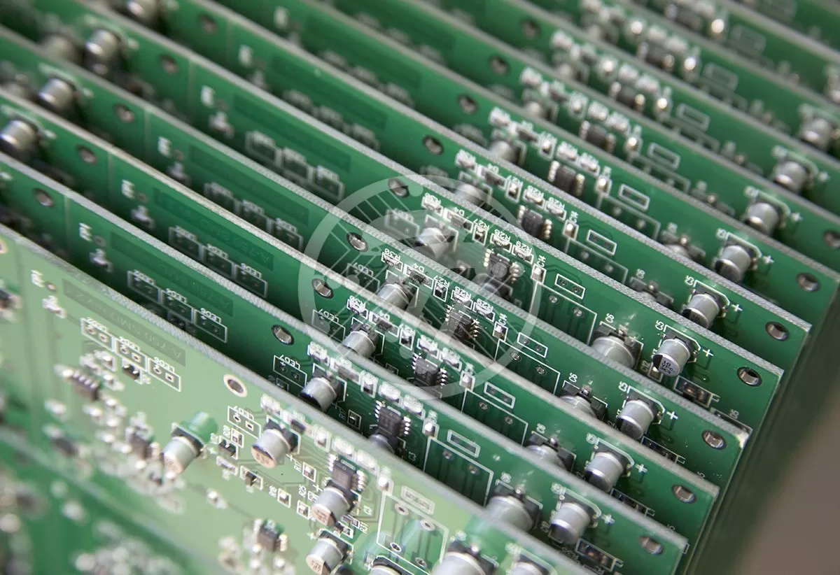
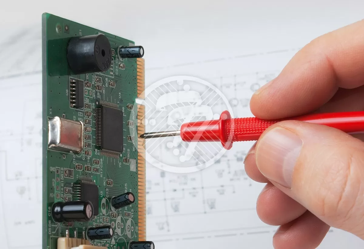
Quality of PCB
If there is one thing that tops the list it is to check for quality standards. This is critical both at the prototype and the design stage as small mistakes can lead to failure of the entire project.
PCB Manufacturing Cost
It is important to shop around when it comes to PCB fabrication so as to get competitive rates. It is also important to remember that while experienced designers may command a premium, quality and price aren’t always directly proportional. The vendor should also be able to provide you instant quotes so you do not waste time going and forth wasting time at the quote stage itself. Check out Some of the biggest influences that affect PCB Manufacturing Cost.
Speed
With most PCB projects having stringent deadlines, speed and timely deliveries are of essence. It is crucial, therefore, to check for turnaround times and delivery schedules. Often times price can be competitive at the cost of delivery schedules, hence this is an area to watch out for. Overall the responsiveness of the vendor is key criteria that goes towards making the right choice.
Minimum orders
When it comes to PCB Projects, particularly the prototype ones, order quantities are of essence. It is important that the manufacturer be able to cater to your minimum order requirements since different companies may operate at different minimum order benchmarks.
Customization
When it comes to PCB requirements, there is clearly no one product that can fit all requirements. Basis the specifications the PCB can vastly differ. It is therefore important to choose a vendor that can customize the PCB to your unique requirements. Choosing a vendor who has the requisite experience in your industry can therefore make a whole lot of difference.
PCB Support
It is also important to note the kind of support that the vendor can offer. For example, if the vendor has the expertise to review the design and point out any errors, it can save you from a whole lot of costly mistakes later. The vendor should also have online management and reporting tools that enable you to easily track the progress of your project as well as upload design documents and bills of materials. The vendor should also be able to support the file formats provided by you.
In choosing the right PCB Assembly Manufacturer, therefore you must ask him the following questions:
- What is their industry experience- This will give you a fair idea of the kind and range of work they may have done as well as their ability to adapt to different requirements.
- What are their certifications- Once again these will help you assess their compliance with quality standards.
- How strong is the customer service team and where is it located- This will help you assess the level and quality of support that the manufacturer will be able to offer you.
- Where do they manufacture the PCB boards- This will help you determine if the PCB manufacturer does really have manufacturing capabilities or if he is only a broker trying to pass off as a manufacturer. You should also determine if they have onshore manufacturing as that will help manage complexity, costs as well as any delays in dealing with an overseas provider. The location of the manufacturer will also help in terms of:
- Individualized attention
- Product control
- Quick reaction time
- Face to face collaboration
There is no substitute to robust research when it comes to choosing the right supplier. Beginning with research on the net, to asking the supplier relevant questions as also seeking recommendations all go towards making the right choice. It is always a good idea to check for the vendor’s list of clients to be able to seek relevant recommendations so that you are able to base your decision on real experiences of other clients and not on hearsay.
At Technotronix, we are fully equipped to handle your PCB manufacturing requirements. With over 4 decades of experience in PCB manufacturing as well as assembling PCBs with differing levels of complexities, we follow industry best practices to ensure we deliver cutting-edge products. Our team of experts and state-of-the-art equipment ensures that all our PCBs meet the industry standards of quality and testing. It is our vast portfolio of satisfied clients that stand as the biggest testimony to our success. In case if you have any questions, please feel free to contact us via email at [email protected]