Why PCB Post Cleaning After the Rework Process is important?

By | Date posted: | Last updated: December 11, 2025
pcb-manufacturing

There has been a lot of talk around the “no clean” process when it comes to PCBs. The reasons for choosing the no clean process are many- beginning with reduced cost per assembly, reduced cycle time as also reduced material handling defects. In addition no clean also comes with the added benefits of reduced cost of cleaning that accrued from reduced floor space, water, chemicals and more.

However PCB cleaning is important on many counts, most important being its functionality. In case any residue remains it can prevent the circuit from functioning properly. The other reason is incompatibility with downstream processes on account of no cleaning. For example a thorough cleaning process is required before an even distribution of coating is possible. Coating without a cleaning process can result in adhesion and reliability issues.

Some of the other reasons that favour the PCB cleaning process:

  • Flux residues cause conformal coatings to fail.
  • Flux residues make visual QC inspections hard to do
  • Flux residues on high-voltage systems is a major issue
  • Flux residues make the process of troubleshooting extremely hard

Once you have decided that you need to go clean after the PCB Assembly Rework, the cleaning process needs to be consistent. There are tools that can be used to test the cleaning process efficiency such as ionic contamination testers for on-site testing.

With electronic components getting more and more thin, a major issue however that needs to be guarded against is moisture sensitivity. In cases where water soluble fluxes are being used or there is flux residue remaining and washing it off is a necessity, what is important is proper drying so that the components are protected against moisture and thereby damage. In fact not just cleaning and drying, there is also an increasing need of a baked out procedure.

IPC-1601 offers complete guidance when it comes to bake out tables. The amount of open time that the board can be without baking is really determined by the environment the board is in. The other factor that determines whether a bake up procedure is required is whether an on-line or batch washer was used for cleaning. Also in case there are areas that can entrap water, a bake out process becomes necessary. Moisture is known to be entrapped inside connector pins, under ICs and other such components. If a bake out process isn’t performed what is likely to happen is that the trapped moisture can impact reliability as also skew test results in case of electrical tests. The need for bake out is also impacted by the type of drying system used. Typically, if an air knife is used, the chances of requiring bake out are high. On the other hand, if convection heat technology is used, the chances for requiring bake out as significantly lower.

The dry out process also depends upon the type of material used for making the PCB. The thermal profile of the wash process also affects how much water will be absorbed by the PCB. The more hydrophobic the board, the less water it will absorb. If the wash systems are so chosen that the board temperature increases steadily, the board is likely to become more hydrophobic.

This is not to suggest that over baking should be indulged at any time. In fact overbaking has a whole lot of issues of its own and can lead to defects in the assembly. With oxidation rates increasing with heat, it can impact the wetting action of the solder.

Is it possible to measure PCB Water Absorption?

Indeed it is and one of the simplest ways to do that is to weigh the board before and after drying. The difference in weight can in fact be used to arrive at optimal pre-bake temperatures.

To ensure that the absorbed moisture is fully taken care of, the boards are best left stacked in a rack for as much as four hours depending of course on the thickness of the board. They are best not stacked one on top of the other as that makes the drying process difficult. Post the drying process the board needs to be stored carefully in a bag or dry box. The bag needs to be vacuum sealed so that relative humidity is low.

In case baking out is required after cleaning it needs to be done for a period of 2-4 hours at a temperature of 105 degree Centigrade. Alternately a 65-degree temperature is also ideal if the process is done for 8 to 24 hours.

Despite increasing “no clean” claims, easy to clean fluxes and solders, therefore are the need of the hour.

With having a combined extensive year of experience in PCB fabrication, PCB prototyping, PCB assembling and PCB rework, TechnoTronix has created a strong customer base for varied industries to shape up new trends for PCB manufacturing across the globe. Drop an email to [email protected] to get proper consultation or share your requirements to get a perfect PCB with a cost-effective strategy, or give a call 714/630-9200!
Reduce the cost and make PCB manufacturing process faster using DFM

By | Date posted: | Last updated: December 11, 2025
PCB DFM

DFM or Design for Manufacturability, is a process of arranging the PCB layout such that future issues with the fabrication and assembly process of the PCB are minimized. DFM therefore can be said to comprise of both Design for Fabrication as well as Design for Assembly.

Till some time back DFM was thought to be a domain of operation for either the PCB fabricator or the assembly engineer. However increasingly DFM is becoming an essential component of the pcb layout Flow. Not without reason- primary among them being:

  • The reduced cost of finished PCBs
  • The possibility of design failure
  • Maintaining the overall design intent

While in the short run, designs that do not have the cost of checking for DFM defects are seen to be cheaper, there is a long-term price to pay. To ensure that a design that has DFM issues comply with the manufacturing process can turn out to be far more costly. If the issues were detected in the pcb layout stage, they could have been corrected at a far lower cost. In fact with high speed PCB in particular, lack of communication between PCB designers and the manufacturing team can lead to a whole lot of costly failures during manufacturing. Added to this there is also the aspect of time to market since quality products are often taken for granted and being the first to take these quality products to the market offers the real competitive advantage.

There are a number of typical DFM issues which can escape detection in the CAD system but can lead to failure in the real-world scenario.

Some of these typical PCB DFM issues include:

  • Acid Traps- Acute angles that allow acid to build up in the fabrication process
  • Slivers-Wedges that can peel off and expose copper
  • Starved thermals-Isolated plane connections
  • Missing clearance pads
  • Copper that is too close to the edge of the board
  • Missing solder pad masks

The following example scenarios can further help clarify the importance of PCB DFM:

Scenario 1
A certain PCB designer reduced the pad size in order to match the trace width. This seemingly innocuous step however led to a number of complications as the reduction violated the IPC rules. This in turn led to the issue of tombstoning where one end of the component was detached from the copper pad and started to resemble a tombstone, leading to a reduced yield.

Scenario 2
Solder masks not used in between pins by mistake by the PCB designer resulted in solder shorts between the pads of the filter. Also the use of vias extremely close to the pads caused the solder to wick and cause tombstoning. While in this case a recommended land pattern from the manufacturer was used, the recommendations however weren’t for production but for low volume prototyping.

Both the above examples could have benefitted from DFM to avoid costly mistakes at the manufacturing stage. In fact that is the very premise of DFM- that it helps designers design a product and help manufacturers figure out how to manufacture it, while keeping a close eye on the product costs. DFM is known to improve the product’s produceability, testability, inspectability, designability and serviceability. PCB Manufacturing costs can be reduced extensively if the product design does not have to be altered at the mass production stage. In fact the cost to change the design is said to be inversely proportional to one’s ability to change over time. This is what is popularly also known as the Design Dilemma. DFM on the other hand addresses products costs early instead of having to do expensive reiterations in product designs at later stages.

Doing a DFM analysis until some time ago was extremely costly with both the software and the hardware coming at a high cost. Its rate of adoption, therefore, was extremely low. These days, however, with more and more DFM tools being made available at low price points, it is far easier to deploy them. They are also far easier to use by the design engineer even though he isn’t the manufacturing expert. In fact they can even set different sets of rules for different manufacturers.

The key check for a good DFM is that it ensures that the design performs well and that it can be manufactured without adding to either the cost, risk or the time of manufacturing, all of which are crucial for its success. For the same, DFM relies on reducing the number of parts as well as their assembly time. In fact the emphasis is on making simpler designs that focus on both quality and reliability. Companies using DFM also have lower capital equipment cost as they typically land up using their machinery more efficiently. With shorter production times as well as fewer later stage engineering changes, DFM is clearly the need of the hour.

At Technotronix, we are fully equipped to handle your PCB manufacturing requirements. With over 4 decades of experience in PCB manufacturing as well as assembling PCBs with differing levels of complexities, we follow industry best practices to ensure we deliver cutting-edge products. Our team of experts and state-of-the-art equipment ensures that all our PCBs meet the industry standards of quality and testing. It is our vast portfolio of satisfied clients that stand as the biggest testimony to our success. In case if you have any questions, please feel free to contact us via email at [email protected]

10 Simple Ways To Speed Up & Optimize PCB Troubleshooting

By | Date posted: | Last updated: December 11, 2025
pcb-troubleshooting

Due to the ceaseless modernization in technology trends, PCB assembly is more complex and intricate in present times than ever before. With this, the PCB troubleshooting is becoming one of the monumental pursuits that accounts for specific expertise, technology and R&D. Fortunately, there is no need to fluster or ruffle as there exist some simple ways for PCB troubleshooting that can help speed up to detect, verify and test the troublesome components and features in a damaged Printed Circuit Board. The below content will drive you to the simple hacks, yielding techniques and easy ways to optimize and speed up the PCB troubleshooting.

It turns out to be more challenging when troubleshooting a multilayer PCB that is well complimented with scrupulous factors like signal analysis, size, types of components and number of layers. Some complex PCB’s require particular mechanized equipment for PCB troubleshooting, while in many cases, the PCB rework and repair is executed with basic electronic instrument for smooth mechanism of current, signal and traces through the circuitry.

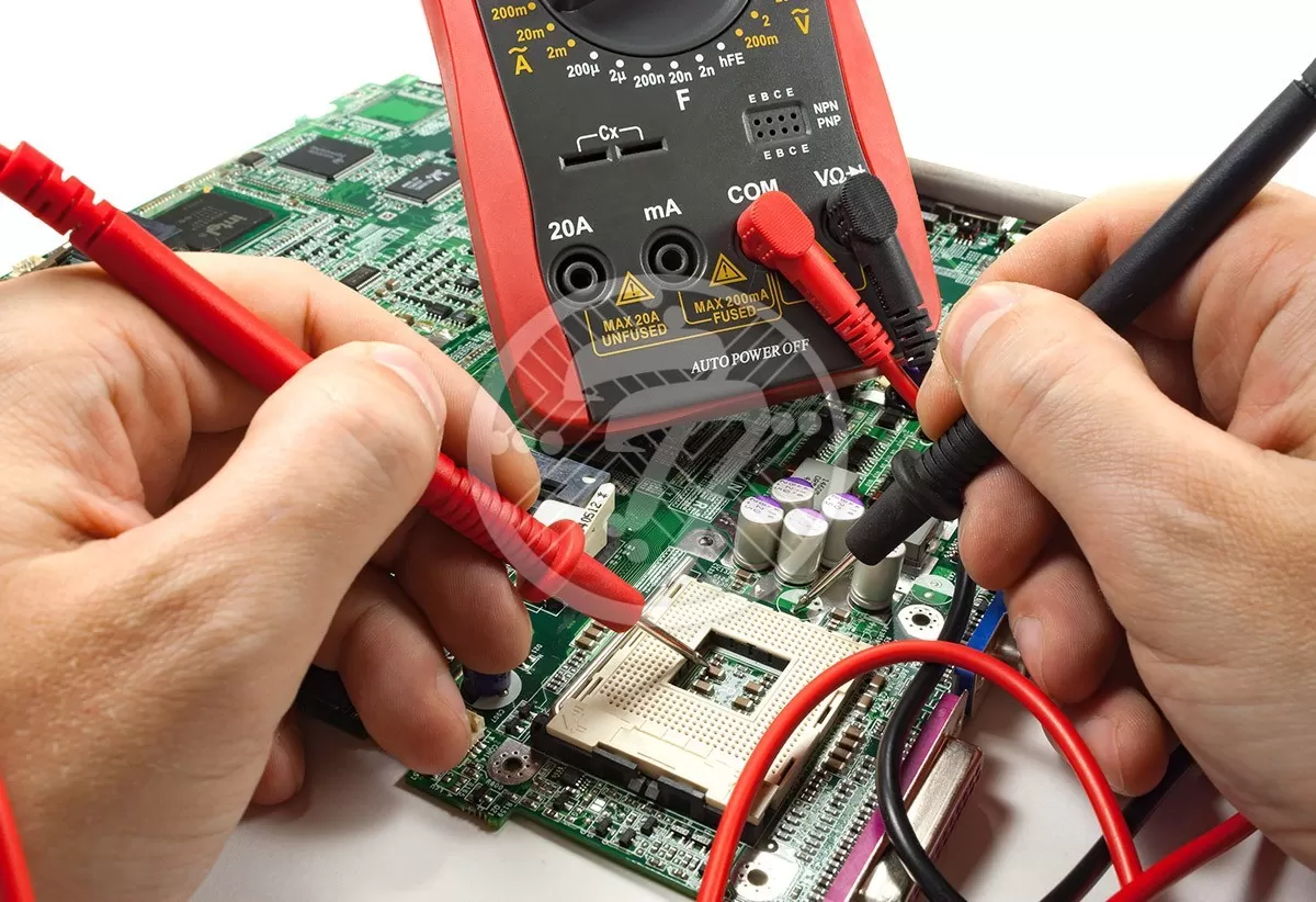
Some common tools for PCB troubleshooting majorly used by PCB manufacturer includes Multi-meter, LCR meter, Logic & power supply analyzer and Oscilloscope that have specific foundation to deal with the complexities and need to probe into the roots of operational behaviour of the affected circuitry. Let’s roll up our sleeves and move on to further readings on ways to simplify troubleshooting the defective single layer PCB, Radio frequency PCB, digital/analogue mixed PCB, rigid flex PCBs and many more.

Top ways to speed Up & optimize PCB Troubleshooting are as below:

  • Magnified and thorough Visual Inspection technique

    – The simple method to identify and locate the PCB damages is tracked and controlled through a This method helps to detect the traces that are overlapped, high sign for overheating, cracked up or damaged components and lacking components on the PCB. In many cases, few burnt or bulging components can be immediately found through magnified Visual Inspection technique.

  • Discrete Component Inspection

    – is one of the concentrated methods for PCB troubleshooting that helps to sharply test each and every component individually. This type of testing is performed with the help of varied tools. With using LCR meter or a Multimeter, one can test the piece by piece values of transistor, capacitor, resistor, inductor, LED and other active components. The component is stated well that possess equal to or less that standard component value. On the other hand, either the solder joint is detected faulty or the component is stated bad if the component value is indicated as higher than that of standard component value.

  • Nodal Analysis

    – Another option that allows a unique comparison between measure of current and voltage by applying power to every component individually is.

  • Physical Inspection

    – A step ahead to a visual inspection technique, is conducted with the power exerted on a circuit. Without using the Thermo Graphic Camera that proves to be pretty expensive, hot spots are detected with the technique to touch the surface of a printed circuit board along with the components on the circuit board. The detected hot component is then cooled with the help of compressed canned air to lower the temperature in order to test the circuit mechanism.
    No doubt about Physical Inspection to be one of the easy and effective way to optimize the PCB troubleshooting, but at the same time it is also considered a dangerous method that needs a lot of precautions to be taken. This method should only be applied on the lower voltage circuit boards. On the other hand, touching powered circuitry and varied components on the PCB, brings variation in the impedance of the circuit in turn changing the system behaviour. Due to such alterations, it becomes effortless to locate the affected circuit that calls for the additional capacitance to operate smoothly.

  • Integrated Circuit Analysis

    – Another simple method to optimize PCB troubleshooting includes. Some IC’s are identified by analysis through Logic analyzer or Oscilloscopes while many IC’s are simply detected by their markings. What make it more and more challenging are the special types of IC’s in varied configurations in addition to the complex PCB Layout. Herein, one of the simple ways to deal with damaged PCB is to compare the behaviour of the affected circuit with that of good circuit to track the anomalous behaviour on the circuitry.

  • Analogue Signature Analysis

    – When PCB documentation or its component signature has been lost, is one of the effective techniques of PCB troubleshooting to test the unpowered, dead or faulty PCB’s.

Other ways to speed up and optimize the PCB Troubleshooting

  • Functionality Testing
  • Using a PCB troubleshooting software
  • Checking of solder joints

Lastly, some more simple hacks to effectively diagnose the faults in PCB:

By alternating the voltage, one can test the unknown high pin count. Also use required devices like Multimeter to get all the signatures, inductance of each component and voltage resistance current in order to compute and compare it with the signatures of defective PCB.

Technotronix is an experienced professional to proffer optimized PCB troubleshooting, PCB rework and PCB repair services. With having a wide customer base from different industries, has made it possible to tune up, modify and alter the defective, dead and out of order PCB’s. At the prima facie, we initiate the PCB troubleshooting project with a smart plan for all the issues to be focused on. Some of these include time taken, material cost, type of inspection required and the need for a Pb-free PCB solder. After the parameters are identified for PCB troubleshooting, Technotronix takes a next step towards a well-defined PCB rework process using upgraded technology. Check out PCB Assembly rework to track down more details on our PCB troubleshooting services. To get your ‘out of order’ PCB’s repaired or reworked, feel free to drop a mail or start a talk with our PCB experts!

Why Bill of Materials (BOM) is important in PCB Manufacturing process?

By | Date posted: | Last updated: December 11, 2025
pcb-manufacturing

The importance of an efficient production plan cannot be overstated as it goes a long way in optimizing production as well as balancing production lines. The need of the hour therefore is a robust design data comprising of pcb layout data, Bill of Materials popularly known as BoM as well as product references.

In fact the entire SMT manufacturing process is BoM driven. This is because the functioning of the PCB is dependent on the components listed in the BoM. The use of the right components in turn is critical to the functioning of the PCB. Any PCB Assembly order, therefore needs to be initiated with a bill of materials. Not only does the BoM carry the list of components but also their placement on the printed circuit board. The BoM, in turn, allows the procurement specialists to figure out the right distributor for the components as also look for cost effective price points. There is a chance that some components may not be available and therefore it gives the procurement specialists an opportunity to look for alternative distributors, so that work can proceed seamlessly.

A detailed Bill of Material with specifications related to item number, description of the part, name of manufacturer, quantity and more, therefore comes in extremely handy. Not only does this ensure quality, it also ensures that the PCB manufacturer can follow the delivery deadlines without any hiccups. In case of turnkey assemblies, it is also essential to mention names and details of both the distributors and manufacturers. In fact multiple distributor names can help the procurement process and can ensure that no time is lost in case a specific distributor does not have the parts readily available.

An optimized component list allows the assembly to be well planned with clearly laid down scheduling steps. This in turn ensures that the PCB is produced with zero errors. On the other hand absence of an effective BoM could mean a whole lot of revisions culminating into delays in delivery.

It is common practice for the manufacturers to provide a template for a sample BoM so that all the necessary information is captured and so there is no room for any ambiguity. Often times support for both explosions and implosions is also included in the BoM. While explosions refers to displaying the components of the assembly, implosions help see where is specific part is used and to determine which sections are then linked to any part which is at risk. Hierarchical BoMs therefore come in handy to study the entire structure.

Also Checkout : The bill of materials in PCB design

Here are some aspects to be especially mindful of, while creating a PCB BoM:

1. Be extremely thorough – Ideally a BOM should help the manufacturer create your PCB from scratch. If you have received a BoM template from the PCB manufacturer to ensure that you spend enough time completing it and providing all the requisite details.

2. Indicate where you can allow flexibility – Odds are that there could be some parts that are critical where you would want the PCB manufacturer to follow the approved vendor list strictly. While there could be others, which are non critical and therefore they can be optimized for cost.

3. Ensure that the parts are available – While listing the parts in a PCB BOM, a quick check on whether the parts are readily available will go a long way in ensuring seamless production

4. Decide how many levels the BoM requires – It is important to determine whether the PCB BOM should be single level or multiple level.

5. Document changes – There are likely to be changes in the PCB BOM from the prototype stage to when it is actually produced and these changes need to be recorded.

Consider the Bill of Materials as your shopping list, stepping out without which is likely to lead to inadvertent omissions and costly errors. The thumb rule clearly is to do a thorough assessment of your needs and build the BoM around it.

Technotronix has a combined and extensive years of experience in PCB manufacturing, PCB assembly, PCB fabrication, PCB prototyping and PCB engineering. We offer high end customization to address the exact needs of electronics manufacturers. Please feel free to contact us to get consultancy, quote or to get updates on our recent project. Get a quick quote!