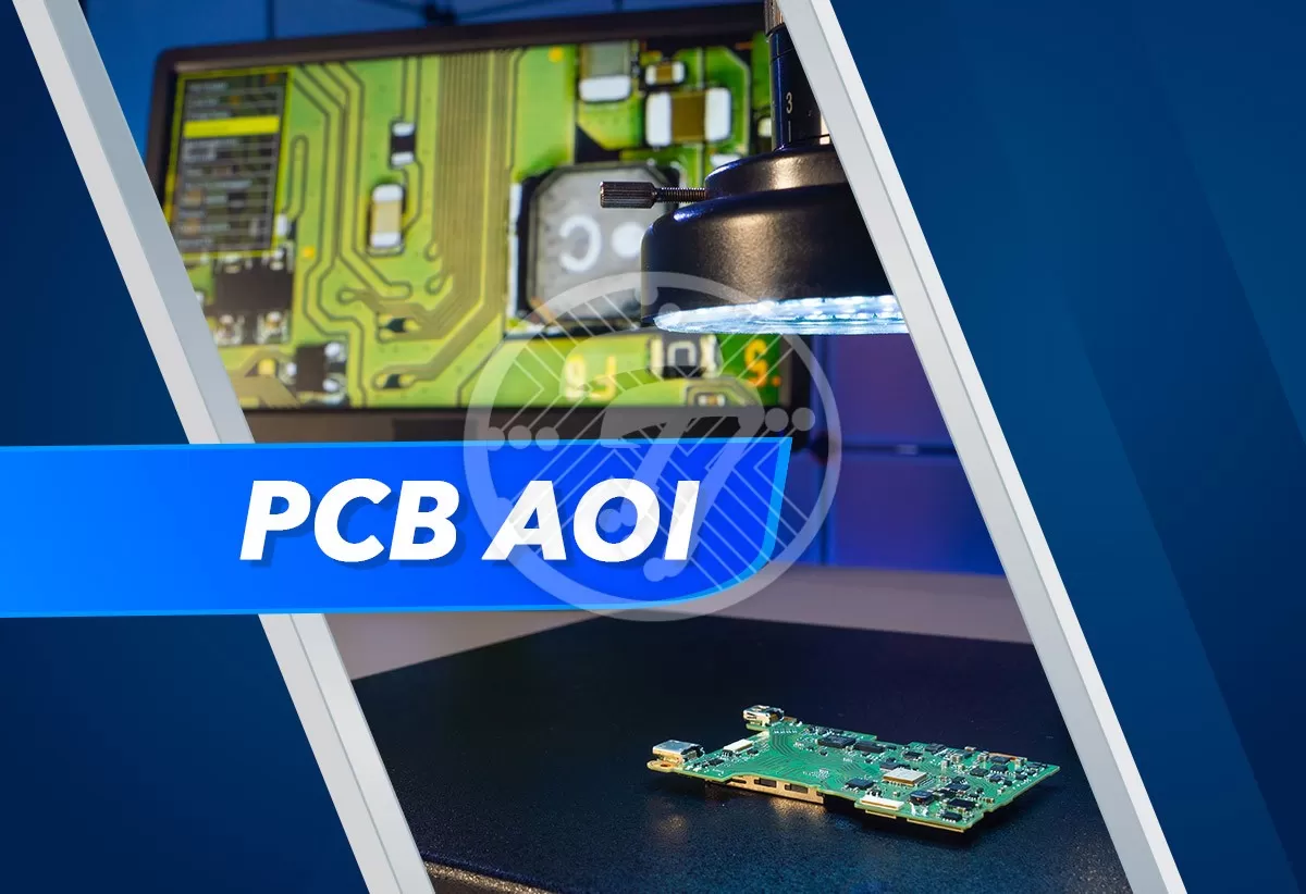
Best practices for avoiding solder balls to ensure flawless SMT manufacturing!

By | Date posted: | Last updated: September 27, 2022
SMT manufacturing

A big issue when it comes to Surface Mount Technology (SMT) manufacturing is the formation of solder balls. These can be caused on account of a wide variety of reasons and can result in several issues even causing the end product to fail. Let us look at what exactly solder balls are and importantly what are the ways to avoid their formation.

What are Solder Balls?

Essentially these are balls of metal alloy that are formed on the surface of the PCB once the soldering process is completed. The formation of solder balls, impact the functionality of the PCB. They can even impact the quality of the component joints especially if they are large in size. Even more damaging is the fact that if these solder balls roll onto other board parts they can cause shorts.

Some of the reasons that lead to the formation of solder balls include:

  • High humidity
  • Excessive flux in the solder paste
  • High temperature or pressure during the reflow process
  • Improper cleaning post flow

Top ways to prevent solder balls

Some of the ways to avoid formation of solder balls include:

1. Ensure there isn’t too much moisture

You need to take care that the board is free of moisture. For this, it is important to store the PCB in a dry place. Also it is important to dry the board before production with anti-static cloth. Also, baking the boards at 120 degree Celsius works for four hours works well to ensure that excess moisture evaporates.

2. Choose the right solder paste

Solder paste that is high on metal content has fewer chances for solder balls to form. It is also important to ensure that there isn’t too much flux in the solder paste. While Flux can be used to prevent oxidation however excess of it can lead to a structural collapse.

3. Preheat the PCB

It is important to preheat the boards so that they are as close as possible to the oven’s temperature. This will ensure that the solder melts evenly.

4. Ensure that the solder mask is in place

Ensure that the solder mask is in place and that the solder paste is used properly so that there are no gaps between the traces & the pads. Using high quality equipment as also keeping the rate at which the board is preheated, low are other ways to ensure that the solder spreads evenly.

5. Ensure that PCB mounting stress is under control

If there is a lot of stress on the board when it is mounted, the traces & pads can stretch or condense. If there is too much inward pressure the pads will be pushed closed. On the other hand, if the pressure is too much outwards the pads will be pushed open.

6. Ensure pad spacing is correct

Incorrect pad spacing can lead to issues in solder pooling. Incorrectly placed pads can, not only cause solder balls to form but also for them to fall out & cause shorts. The pads must therefore be placed optimally.

7. Ensure that the stencil is clean

It is important that the excess solder paste is cleaned off the stencil. Any excesses can lead to formation of beads or balls. In fact after each round the stencil should be cleaned. While this may involve time, it will ensure that it does not lead to costly errors.

8. Ensure that the stencil dimensions are correct

It is important to choose a SMT stencil with the right thickness. Stencils that are too thick do not work well. Additionally, stencil opening ratios & shapes need to be paid due attention to.

To sum up

Solder Balls can lead to a wide variety of issues. However, fortunately with some basic precautions you can prevent their formation. It is imperative that you look at your production process step-by-step & ensure that you take the necessary steps so that the formation of solder balls can be prevented. With the above tips you can ensure that the risk of solder ball formation is minimized. It is important that you choose the right electronics contract manufacturer who has the requisite experience and stringent quality control measures to offer high quality PCBs.

At Technotronix, we are fully equipped to handle your PCB manufacturing requirements. We have over 40 years of experience in SMT PCB assembly. Our team of experts and state-of-the-art manufacturing facilities ensure that all our PCBs meet industrial standards. If you are looking for high-quality SMT PCB solutions, you can submit your requirements via PCB SMT assembly quote form. Also, if you have any questions, please feel free to contact us via email at sales@technotronix.us

Find out what causes PCB tombstoning and how to prevent it!

By | Date posted: | Last updated: September 15, 2022
PCB tombstoning

If there is one place you do not want a tombstone, it has to be in your PCB. As its name suggests, tombstoning refers to those large, slanting slabs that you see in a cemetery. Except that in your PCB, the tombstoning is caused by a surface mount passive component such as a resistor or a capacitor that partially lifts from a pad and stands on end and resembles a tombstone. This happens frequently, especially when you have two-pin, passive components like resistors, capacitors and inductors. However, tombstoning isn’t limited to passive devices alone.

Reasons for PCB Tombstoning defect

Some of the reasons that cause tombstoning to occur include:

  • Different wetting speed during soldering leads to imbalance in torque.
  • Solder pads that aren’t designed properly.
  • Erroneous placement of components.
  • Inconsistency in pad size.
  • Reflow oven temperature not being even.
  • Chip being placed parallel to the reflow oven.
  • Varying heating capacities of PCB materials.

Ways to prevent PCB tombstoning

The good news, however, is that with the right Design for Manufacturing practices, tombstoning can be prevented. Let us look at some of the DFM (design for manufacturability) best practices that can help prevent tombstoning:

Footprint Pad Size

It is imperative that the pad size for the small, passive components is accurate. In the absence of this, the thermal mass of the solder joints will be affected. If the pad has less mass, it is likely to cause the solder to reflow faster than the larger pads. It is important, therefore, that in building the CAD footprint pads, industry standards be strictly adhered to.

Footprint Construction

Another area to pay due attention to includes the footprint of the passive part. It is important that the part is centered on its origin. The spacing of the pads is also extremely important. The manufacturer’s recommendations as well as the industry standards need to be meticulously followed.

Trace routing and power planes

It is crucial that the trace routing is balanced. For example, if one pad is connected with a thin trace & the other is connected with a thick trace, the imbalance thus caused will be fatal. In such cases the additional metal will work as a heat sink & the solder paste on one pad will melt slowly than on the other.

It is also important to remember that embedding a pad within a power plane can have difficult consequences. The routing between the pads needs to be balanced. It is also necessary to use thermal ties when a pad is connected directly to a metal plane.

Additionally, it is also important to remember the following aspects:

PCB Finish

For small component sizes such as 0201 or 0402, it is best to avoid traditional hot air solder leveling or HASL, as it is popularly referred to.

Solder Mask Thickness

It is important to assess the solder mask thickness carefully so that while it masks for oxidation, it does not restrict solder movement.

Copper Coverage

Unequal copper coverage can lead to uneven heating thereby leading to tombstoning.

Stencil Design

A proper PCB stencil design will ensure that there is just about adequate solder paste as too much solder paste can lead to high torque. Also the component-to-paste overlap needs to be appropriate. Too little of it will lead to issues in adhesion. On the other hand, too much of it would lead to solder beads appearing.

PCB Testing

Importantly, robust PCB testing is extremely important so as to eliminate any costly errors at a later date. Each component needs to be tested so that the functioning of the PCB is not compromised. Some of the popular tests include:

  • In-circuit testing
  • Flying Probe testing
  • Automated Optical Inspection
  • Burn-in testing
  • Other functional tests

To sum up

The above best practices will ensure that you avoid tombstoning in the small, passive parts. Additionally, it is extremely crucial that you make the choice of the right contract manufacturer who is equipped with industry best practices The right contract manufacturer will be able to create the right CAD footprint models as also ensure that the component placement and the right routing recommendations are made.

TechnoTronix is an ISO 9001:2015 certified company that delivers one-stop PCB manufacturing services with specialized support, reliable testing, and multi-functional features. In case you have any questions, please feel free to contact us via email at sales@technotronix.us or call us at 714/630-9200.

Importance of PCB insulation in PCB manufacturing!

By | Date posted: | Last updated: September 8, 2022
PCB insulation

While the use of PCBs is ever increasing, what is also increasing is the heat that is generated by them. In fact, a large percentage of printed circuit boards are known to fail on account of the heat. The need to insulate PCBs is therefore paramount. Insulation helps provide protection against changes in temperature.

PCB Insulation is the process of using a dielectric material to offer the much-needed coverage that does not allow for contact with electrical conductors and helps separate & isolate conducting elements & layers. When the PCB is rightly insulated it also protects the non-conductive metals from corrosion.

Major objectives served by insulation of PCBs

The major objectives served by insulation of PCBs include:

  • It ensures there is no signal interference between adjoining layers.
  • It supports voltage integrity.
  • It ensures suitable thermal delivery & aids in PCB operation.
  • It helps maintain adhesion during the cycling of assembly temperature.

Categories of insulation coating materials

Some of the insulation coating materials commonly used include:

Epoxy Resin Coating

This is known for its strength as also its resistance to corrosion, moisture & temperature. However, it is important to remember that this isn’t too suitable when it comes to cold conditions, as it is known to shrink. Additionally, any alterations are difficult as it needs to physically stripped and can cause damage.

Polyurethane Coating

This coating is known for its durability & resistance to acids. However, the flipside with this is that rectifying any PCB defects with a polyurethane coating is tough.

Organic Silicon Coating

This is highly suited for high-circuit PCBs. The fact that it is pliable & is resistant to moisture & heat adds to its advantages. On the other hand, however, it is not known for its mechanical stability as well as its inability to resist corrosion.

Parylene Coating

This works very well for high frequency PCBs especially as it provides total cover. The only thing that stands in the way of its wide application is its cost.

Acrylic Acid Resin coating

This coating lends itself easily to any modifications & is also known for its affordability. The additional advantage that it offers is that it is moisture resistant & also dries quickly.

PCB Insulation Materials

Let us also take a look at the commonly used PCB insulation materials:

FR-4

Fabricated from entwine fiberglass, it is known for its flame-retardant coverage. The fact that it is also cost effective explains its widespread use.

FR-2

A blended material fabricated from paper & plastic carbolic acid; it is known to be long lasting and works well for single sided PCBs. It is also extremely cost effective.

Radio Frequency Coating

As their name suggests they are well suited for PCBs that enable high radio to frequency & find wide use in in-flight & other such electronics.

Flex

For flexible circuit boards, Flexible and thin plastic is typically used as substrate. Flex circuits are often protected by PCB insulation coating spray.

Metal

Metals are conductive in nature hence this may seem like a strange insulation option. However, metal substrate works well for insulation of PCBs. Being good conductors of heat & electricity, they ensure the current is handled without burning or breaking it.

Factors to be considered for material selection, Insulation thickness and layer signals

If thin insulation is used, it helps to have the ground layer adjacent to the signal layer to reduce EMI. In case of a thicker dielectric however, two signal layers can be routed on adjacent layers, provided traces on one layer is routed perpendicularly.

Type of board

For most board types, FR4 works well. However, especially for high-speed boards, controlled impedance can be a factor. In such cases the height of the PCB insulation is important.

Overall board height

The number of layers, insulation type & board height all go a long way in being able to make the right choice.

Thermal Cycling

Yet another factor is the number of times the board is exposed to high temperatures cycling.

To sum up

PCB insulation goes a long way when it comes to ensuring the durability as well as the integrity of PCBs. With PCB insulation ensuring that heat is channelized away from sensitive components, optimal operation of the PCB & hence of the electronic device is a reality.

Technotronix provides a one-stop solution for PCB manufacturing services with specialized support, reliable testing, and multi-functional features. In case if you have any questions, please feel free to contact us via email at sales@technotronix.us or call us at 714/630-9200.

What makes flexible PCB board the best choice for satellite applications?

By | Date posted: | Last updated: November 11, 2022
Flexible PCB Board

When it comes to satellite applications, the use of flexible PCB boards is only growing! Not without reason! There are a large number of benefits that are pushing industry players towards the adoption of flexible PCBs. From reduced weight to increased reliability, there are a whole lot of advantages that flex PCB offer. Before we look at some of these advantages in detail, let us first understand how a satellite operates:

How does a satellite operate & what is its use case?

The satellite system has 3 main circuitries, namely:

  • Satellite
  • Receiver
  • Transmitter

While the communication between a satellite & transmitter is referred to as uplink, the one between the satellite & receiver is referred to as downlink.

The use cases of satellites include:

  • Disaster risk management
  • Weather Forecast
  • Remote Sensing
  • Geo-Positioning
  • Navigation
  • Telecommunication
  • Emergency Response Monitoring

Satellites, in turn, can be of 3 types, Fixed, Mobile & Broadcast, depending on the services they offer. A Fixed Satellite Service uses fixed receiving stations. These are primarily used in cable TV and internet stations. Mobile satellite services also deal with mobile systems for communication with fleet vehicles. Broadcast Satellite Service broadcasts TV & radio signals.

Given the functions that satellites perform, let us now look at the need for flex PCBs in satellite applications.

Advantages of using flexible PCB board in satellite applications

Reliability

Satellites represent mission critical operations and failure can come at an extremely high cost. It is imperative therefore that the PCB being used is extremely reliable. With flexible PCBs being able to withstand higher stress than rigid ones, they are suited for use in satellites that are subject to harsh environmental conditions. Additionally, Flex PCBs take away the use of connectors, which often cause interconnection failures. You are therefore assured of reliability when it comes to the use of flex PCBs in satellites.

Adaptability

The big advantage that flex PCBs offer is they are extremely adaptable, and land lends itself to shapes that ’t regular. Flex PCBs can fit into different surfaces that they are mounted on. However, this is not possible with rigid PCBs that cannot be used in complex shapes.

Their flexibility also comes in handy when you need extensible parts. With flexible circuits you can make use of expendable equipment without any fear of wear & tear.

Lightweight

With thinner copper layers as well as insulating layers, flex circuits are lightweight and can also adapt to tighter spaces with low bend radius.

While flexible circuits are made out of many materials, Kapton is particularly widely used because of its light weight. In addition, it is also known for its mechanical properties as well as vibration resistance.

While Flex PCBs are therefore well suited for use in satellites, it is imperative that PCB designers take the following conditions into account while designing PCBs for satellites:

Operating Temperature

It is important that the material chosen for PCBs to be deployed in satellites is suited for the harsh operating conditions. In fact, the material chosen should be able to survive in elevated temperatures of 120 degrees Celsius, or more.

Outgassing

When a PCB operates in a high-pressure environment, the gases trapped in the PCB are released. The gas released can condense on other sections and cause operational issues. It is therefore important to choose a material with good thermal resistance so that outgassing is controlled.

Orbital Collisions

With satellites, orbital collisions can be a reality. The PCBs should therefore be able to withstand such collisions. To ensure that, the flexing capacity of the PCBs should be high.

PCB standards for use in satellites

Because of these unique issues, there are specific standards when it comes to space applications. The common standards include:

AS9100

Created by the International Aerospace Quality Group, this standard is useful for creating products for the aerospace industry. AS9100D is the latest standard that the aerospace industry needs to adhere to.

The other standards that Aerospace as well as military-grade PCB assemblies need to adhere to include:

  • MIL-PRF-50884
  • MIL-PRF-31032
  • MIL-PRF-55110

To sum up

Rigid flex & fully flex PCBs offer several advantages over traditional PCBs. Their innovative design, reduced weight and more make them an ideal choice. It not only helps to minimize the size of the spacecraft but also improves reliability.

We have over 40 years of fabricating and assembling a wide variety of flexible aerospace PCB assemblies. With state-of-the-art equipment, we deliver the highest quality boards that you can rely on. Armed with an experienced flexible PCB board manufacturer team that can advise you on industry best practices, what you get when you join hands with us, isn’t just a vendor but a partner who is invested in your success. In case you have any questions, please feel free to contact us via email at sales@technotronix.us.