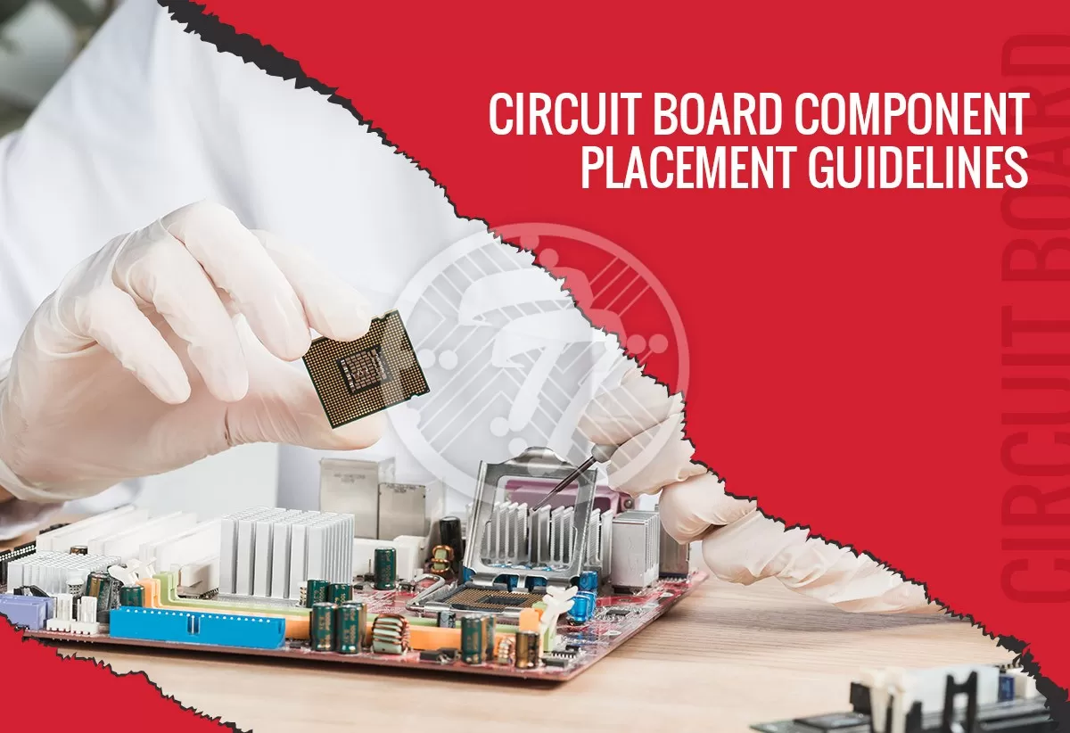
Top signs that indicate that it is the time for a circuit board test!

By | Date posted: | Last updated: August 26, 2022
Circuit Board Test

The flawless working of a PCB is the key to the reliable working of any electronic equipment. It is therefore imperative that you be watchful of signs that indicate that your circuit board is faulty & that indicate that it is time for a circuit board test. Here are the aspects to look out for:

Common signs and causes of PCB failure:

Burnt Components

When the PCB needs to work under extreme temperature conditions, burnt components can be a reality. There are several factors that can result in burning of components, important among them being:

  • Area surrounding the component
  • Shape & size of the component

Overheating of components is a sign that all is not well with the PCB. Not paid due attention to, it can lead to operational issues.

Issues during manufacturing of PCB components

Issues in either the manufacturing of components or their improper placing can result in a number of issues. Some of the common issues faced include:

  • Improper soldering
  • Chemical leaks
  • Poor connectivity between layers
  • Loose components
  • Other human errors

An easy way to check for any issues with SMT components is to conduct a dye- and- pry test. It will go a long way in telling you about the issue & how the device is being impacted because of it.

Environmental Factors

In assembling electronic components, it is extremely important that environmental conditions are controlled. For example, humidity in the room can lead to a wide variety of issues. Similarly dust & heat can impact the PCB, as can issues such as an accidental fall. Some of the other causes that can lead to malfunctioning of PCBs include accidental submersion in water or exposure to lightening, for example.

Also, overtime dirt can accumulate in the PCB & cause it to malfunction as also reduce its lifespan.

Age of components

As components age, circuit boards can eventually fail. In fact as components reach end of life, malfunctioning can increase many fold. Component replacement at this stage may therefore become a reality.

Armed with this information about potential causes of PCB failure, the importance of printed circuit board testing cannot be overstated. Testing can reveal issues that can be addressed through rework & repair.

If you already suspect that your circuit board may be faulty on account of the above reasons, what then are some of the recourses available to you?

What to do in case of a suspected faulty circuit board?

1. If the board’s electronic components are in place, the first thing to do is to test the board with its power on.

2. In case electrical components have not been installed, the power needs to be shut and the connection wires cut, before the board is inspected.

3. It is important to check the circuit board for any visible signs of damage. Signs can include components that are crushed, wires that are cracked, any burn marks or scratches and more. Scratches can damage connections while misplaced solders can disrupt connections or even cause a short circuit. In case such signs are visible there is no need to continue the testing. Instead the damaged parts need to be immediately replaced.

4. Switching the circuit board on & checking for the voltage of all connections with an oscilloscope is an important step. Voltage probes need to be applied to the end of each connection so as to be able to identify the issue.

5. In case connections aren’t conducting the specified voltage, what is indicated is a bad connection.

To sum up

Over a period of time, PCBs can undergo damages that can impact their functionality and therefore the functionality of your electronic device. Timely testing can ensure that the board is repaired or reworked. Of course, understanding the exact issue is the vital first step to be able to make the necessary repair. Knowing the signs of PCB failure can therefore go a long way in ensuring that you take timely action & that the functioning of your equipment isn’t compromised. Needless to mention, that in mission critical operations timely testing & necessary action can be life saving.

TechnoTronix is an ISO 9001:2015 certified company who delivers one-stop PCB manufacturing services with specialized support, reliable testing, and multi-functional features. Our main strength lies in the extensive experience and skilled team of experts to provide error less and lead-free PCB manufacturing solution. You can drop an email to sales@technotronix.us or give us a call at 714/630-9200 to solve your queries or to get a quote.

What are the design considerations and guidelines of round circuit boards?

By | Date posted: | Last updated: November 11, 2022
Round Circuit Boards

Today, PCBs are available in a wide range of shapes, even though square and rectangular PCBs remain the most common. With the ever-developing electronics industry, the one shape that is gaining prominence is round PCBs.

As the name implies, a round circuit boards is a PCB that comes in a circular shape. It is often used in consumer electronics, wearable devices and more.

The advantage with round PCBs is that it offers increased board space. Fabrication of round PCBs however requires a lot of care since it is a complex process. In fact, the routing process of a round PCB requires a lot of time. All of this also has a repercussion in terms of the overall costs of round PCBs.

Types of Round PCB

Round PCBs, in turn, are of different types. These include:

  • Single-sided PCBs
  • Double-sided PCBs
  • Multilayer PCBs

A single sided round PCB comes with one conductive copper layer. This type of PCB is extensively used in low-density designs. Such a PCB has components on one side of the board while there is a conductor pattern on the other side. Such PCBs use either through-hole or surface mount technology.

Double-sided round PCBs have conductive layers on two sides of the board. They are extensively used when it comes to applications such as wearable devices, lighting systems & more.

A multilayered round PCB has more than two conductive layers. Even though they are the hardest to fabricate, they offer multiple advantages including:

  • They lend themselves to higher density.
  • They offer increased board space.

Round PCB Design

It is a given that round circuit boards are more complex when it comes to the design bit. Thankfully though there are few tools available that aid the design of a round PCB. There are several design rules, however, that need to be followed when it comes to round circuit boards. For example, the perimeter of such boards can only be shaped with a straight-line segment. Also, in arranging the lines of the perimeter, a circle needs to be placed on the silkscreen layer. Let us look at some more PCB layout and design rules in detail:

Round Circuit Board Design Rules

  • First & foremost, when using the CAD tool, it is important to draw the shape in the CAD tool.
  • Of course, if the round circuit board is being designed for a high-speed appliance, your choice by default will have to be a multilayered printed circuit board.
  • The power and ground planes need to be defined in separate layers. A polygon editor can go a long way to define the shape of ground or power planes.
  • Some software also offers the option of customizing the power & ground planes.
  • What also needs to be kept in mind is that round circuit boards need panelization schemes for their design.
  • To panelize a round PCB, break routing is widely used. It is imperative that a 10 mm (about 0.39 in) clearance is kept between the round circuit boards. With a larger routing tool, however, the clearance can be increased.
  • As far as the mounting technology goes, both SMT (Surface Mount Technology) as well as THT (Through Hole Technology) can be used to place components, although SMT is better suited.

To sum up

Overall with Round PCBs, designers have a lot of flexibility. The added advantage also is that there is the possibility to incorporate more features as you go along. Also, with the help of CAD tools the designer can add pad shapes in the circuit board.

While such boards are complex to design, the use of the right software can aid the designing process. Following design rules & best practices can also go a long way in making eth process seamless. It is also imperative that you deal with a professional electronics contract manufacturer who is involved in the PCB design phase itself. That way, the manufacturer can assist you with the best practices & point out any design flaws early, so that you do not have to contend with any costly issues at the fabrication stage. Needless to mention that design issues once the board is manufactured can sometimes even lead to irreparable damage to a company’s reputation.

At Technotronix, we are fully equipped to handle your PCB manufacturing requirements. With over four decades of experience in delivering high-quality, on-time, competitive price products, you can rely on us for your PCB requirements. In case you have any questions, please feel free to contact us via email at sales@technotronix.us or call us at 714/630-9200

How to fix common PCB Gerber file issues?

By | Date posted: | Last updated: December 13, 2022
PCB Gerber File

With electronic technology making its way to different fields, the use of PCBs has become ubiquitous. PCB designers & manufacturers are therefore increasingly working towards developing PCBs that are robust & more efficient. This is extremely critical especially when PCBs are being deployed in mission-critical operations where any mistakes can turn out to be extremely costly. One way to do this is to ensure that the Gerber files and the digital blueprints of the PCB are robust. Any errors in the Gerber files can prove to be fatal as they can lead to PCB failure.

Ensuring that Gerber files are therefore complete & accurate is key. Let us look at how to fix PCB gerber file problems.

Here are some of the most common ways to fix common PCB Gerber file issues:

Empty Gerber Files: It may sound incredulous, however, there have been enough & more instances where a Gerber file is an empty or a “zero-byte” file. This can happen on account of many reasons, the most common one being that the data is accidentally deleted. It is therefore imperative that each Gerber File be properly checked before it is sent onwards.

Incomplete Files: If enough attention isn’t paid to the PCB Gerber files, you could have instances where the Gerber file is incomplete. Missing information can prove to be dangerous as it may lead to a board that does not match up to the desired levels.

Improper Labeling: If the labeling of the Gerber files isn’t in line with the established protocols, it has the scope of leading to a wide variety of errors.

Too Many Aperture Lists: It is important that the Gerber File has a single aperture list with all the details. Multiple aperture lists are a source of confusion. It is also important that the format of the aperture list is the same as that of the Gerber Files.

Composite Layer Design Errors: In case composite layers are generated while generating individual layer design specifications, the images need to be combined so that one Gerber file is created for each layer.

Missing Board Outline: Sometimes when PCB Gerber files are generated, the board outline is not produced by default. It is important that the actual bounds of the board edge be described.

Missing Drill files – A drill file is required to create any through-hole footprints that might be present in the design. For software packages where a separate option is required for generating drill files, it is important that it is not missed.

Issues with other design files – It is always good to crosscheck that any revisions that have been made to your design are reflected in the Gerber files, Bill of Materials as well as the Centroid File so that there is no scope of any error.

Vectorized Pads: In some cases, rather than generating the pad as one solid object in the Gerber files, the software may output a cluster of small vectors that together form the pad. It is important therefore that the software is set at generating “ Flash Pads” as opposed to “Vector Pads”.

To sum up

While the good news is that it is easy to avoid Gerber File errors, the bad news is that any errors made can lead to far-fetched consequences; consequences that are expensive, time consuming and that can cost you your company reputation. As they say, it is better to be safe than sorry. It is important therefore that any sources of potential errors in Gerber Files are checked & fully eliminated. Some simple ways to ensure that you avoid Gerber File errors include:

  • Making use of a Gerber file viewer
  • Printing a simple board. This will allow you to see that the specifications are correct & that there are no errors or omissions.
  • Making use of high-definition CAD software
  • Importantly, making use of Quality Control practices throughout the design process.
  • Choosing your PCB partner with care. The right partner will ensure that a rigorous quality assurance process is undertaken. This will include checking the PCB Gerber file thoroughly so that there are no costly errors at a later stage & that the PCB that is manufactured is to the specifications & adhered to stringent quality parameters.

Technotronix is one of the leading providers of PCB manufacturing services to all the dominant industries. With over four decades of experience in delivering high quality, on-time, competitive products, you can rely on us for your PCB requirements. Also, you can drop an email to sales@technotronix.us or give us a call on 714/630-9200 to solve your queries or to get a quote.

What PCB certifications should your manufacturing partner have?

By | Date posted: | Last updated: January 18, 2023
pcb-certifications

When it comes to choosing your PCB manufacturing partner, it is imperative that you are certain that the partner operates within the PCB industry regulations as well as maintains quality standards. The only way you can be sure of this is if you know that the partner has the right PCB certifications as well as robust Quality Management Systems.

QMS

Let us look at the Quality Management Systems first and how they tend to improve operational efficiency:

Some of the advantages of a robust QMS include:

  • It helps improve the overall manufacturing process
  • It leads to repeatability in processes
  • It helps reduce costs
  • It improves the quality of the final product

Established by ISO 9001, the QMS helps in the following areas:

  • It ensures that all the processes follow certain specifications. Besides it also provides a centralized digitized backup for all documentation
  • It also ensures that all the industry compliances are met.
  • It aids in interdepartmental communication and therefore increases efficiency
  • It can track employee performance as also help disburse training modules.

The QMS PCB certifications definitely need to adhere to ISO 9001, however different industries can also have specific guidelines. In addition to ISO 9001, for example, there is also ISO 13485 that particularly focuses on medical devices. This standard applies to a company that isn’t just involved in turn-key operations in the medical industry but also if it is involved in any step of designing or manufacturing medical devices.

IPC

The Institute of Printed Circuits or IPC as it is popularly known as, also provides a number of solutions to the PCB industry & offers research on all aspects of PCB board design as well as manufacturing. Members have access to the following:

  • Industrial research
  • Process development
  • Training guides

These go a long way in ensuring that there are no manufacturing defects in the PCB. Additionally, membership also allows access to industry events, which are a gateway to information on new developments in the industry. An IPC membership, therefore, suitably assures you that the partner adheres to industry norms & therefore acts as some kind of a badge of quality assurance.

IPC-A-610

IPC also generates many standards, the de-facto standard however being the IPC-A-610. This standard is concerned with the right way of soldering as well as assembly. Here are the industries covered under Class 1 to 3 of this standard:

Class 1: General Electronics Products.

This Class refers to products where the tolerance related to defects is considerably higher & the reliability concerns aren’t so severe.

Class 2: Dedicated Service Electronics.

This is a category where the life of the products is expected to be more than those in Class 1. However these aren’t mission critical operations.

Class 3: High-Reliability Electronics.

These PCBs are meant to adhere to stringent tolerances. These are critical operations where any failure can have dire consequences. Some of the industries in which these PCBs are used include aerospace, medical & more

IPC-A-620 or IPC/WHMA-A-620

This is yet another standard that includes areas such as:

  • Crimping
  • Insulation
  • Grommets
  • Ultrasonic Welding & more

Other PCB Certifications

Some of the other important PCB certifications include:

IATR- This is extremely important in the defense industry.

UL 508A- This is used for panels in industrial usage. Some of the areas that fall under UL 508A include:

  • Switches
  • Relays
  • Circuit Breakers
  • Timers

It is however important to remember that the loads connected to this circuitry do not fall under this certification as it accounts only for the panel & the circuitry it has direct control over

To Sum Up

To ensure that your design does not meet any manufacturability issues or worse still that you do not have to face costly errors at a later date, it is very important that the PCB manufacturer is equipped with the right certifications & hence the right experience & expertise to do justice to your project. With the right certifications the manufacturer can ensure that no matter what your design challenges and goals are, they can be met effectively and that your expectations can be surpassed.

As ISO 9001:2015, ISO 13485:2016 & AS9100 Rev. D Certified PCB Company we manufacture high quality PCB with continual improvement in QMS to Achieve total customer satisfaction. If you have any requirements regarding PCB manufacturing or need urgent assistance, contact us at sales@technotronix.us or call us on 714/630-9200.