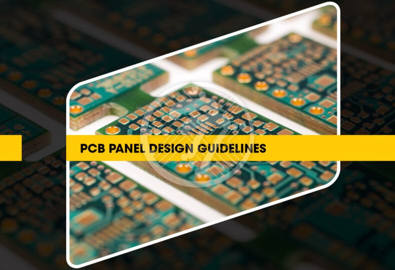
PCB panel design guidelines for trouble-free product manufacturing!

The design of a panel plays an important role in ensuring error free production of PCBs. Each panel comprises of several PCBs that are arranged optimally. With panelization, in turn, you tend to reap a few benefits including but not limited to time saving and cost-effective production, standardization and more. Additionally, the panel provides protection to each individual circuit board. Also, panelization improves efficiency as opposed to manufacturing one circuit board at a time since a few circuit boards can undergo all the processing steps together. It is possible to have a homogenous assembly where the panel has a single type of circuit board. On the other hand, it is also possible to have a heterogenous composition where the panel has different types of standard circuit boards in a certain ratio.
There are, however, some important guidelines that need to be followed when it comes to successful and economical design of the PCB panel.
PCB Panel Design Guidelines
Size of the Panel
Typically panel sizes that are less than 2 inches face an issue when it comes to certain machines such as pick-and place or even AOI. The size of the panel therefore needs to be kept in mind. To address this issue you may need to arrange additional PCBs on the panel or even add some free area around the edges. It is worthwhile to remember that there are also some maximum dimensions to be kept in mind. Typically the maximum dimension is 12″ x 18″ (305 mm x 460 mm).
Form of Panel
If the PCBs have irregular contours, you will be required to add a handling edge around them. This is necessary since machines such milling machines & saws can handle fixed geometric shapes.
Margin for Panel handling
In transporting the panels, it is important that a narrow strip be left free around the edges. For single sided or double-sided structures, the width of the edge can be 12.5 mm while for multilayer boards it can be 25 mm.
Distance between PCBs
It is the separation method that is used that determines the distance that you need to maintain between individual circuit boards. For example, while in case of laser depaneling the distance can be a few hundred µm, for milling, however, it needs to be 2-3 mm.
Distance between cutting edge and components
The distance of the cutting edge from the mounted components is key. Typically the higher the components, more the distance that needs to be maintained. The distance is also dependent on the cutting method & tools used. If you are using a laser beam you can have components at a distance of 100 µm.
Cutting process
The panel also needs to be prepared according to the cutting process being followed. One of the methods is breakout-tabs. If the panel is prepared in advance you can increase the speed as well as the throughput time. Similarly you can also follow the V-Groove method. In this method the panel is cut from above & below removing 1/3 of the material from each side. This method though may not work best for overhanging components.
The other method of separation which does not involve V-Grooves or tabs is laser depaneling. The laser beam requires a cutting channel that is 200 µm wide as opposed to a milling machine where the requirement is between 2000 and 3000 µm. On account of the saving, you can have more PCBs per panel. Not only do you tend to save on the material, but you also ensure that the processing of the panel is far more effective.
To Sum Up
When it comes to the design of the panel, the above factors play a critical role. In turn, these impact the quality as well as the cost of the PCB. While the design of a PCB panel is complex, taking into account numerous factors, a professional PCB manufacturer is equipped with the necessary experience & expertise as also with industry best practices to ensure that the most optimal design is chosen that has an implication on:
- The quality of the PCB
- Its cost
- Overall profitability of the project.
Technotronix provides a one-stop solution for PCB manufacturing services with specialized support, reliable testing, and multi-functional features. In case if you have any questions, please feel free to contact us via email at [email protected] or call us at 714/630-9200.


