Top Causes of Warpage in PCB Assembly Process & Their Prevention Measures!

With the miniaturization of electronic devices, the use of thin PCB circuit boards and small components is in vogue. However, the use of thin multi-layer PCBs with small SMT components also brings some issues in its wake. Typically, such PCBs suffer from warpage in the PCB assembly process that impacts among other things, its yield. Besides, excessive warpage also leads to the quality of the paste printing being affected. Warpage also affects the formation of solder joints during the reflow soldering process.
Before we get to the solutions that can help control warpage, let us have a quick understanding of what warpage really is.
What is PCB Assembly Warpage?
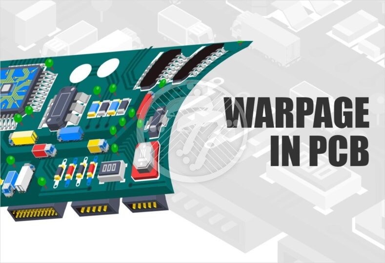
Typically, all parts of the Printed Circuit Board should be in contact with the surface. However, sometimes on account of various stresses this does not happen. What we have is a condition where some parts of the PCB bend upwards and some downwards resulting in positive and negative curvature. Sometimes the bend may be along the axes of the board or along the diagonals. The board can sometimes also develop a twist. All these are examples of PCB warpage.
Causes of Warpage in PCB Assembly
- Built in stress on the copper film causes the boards to warp. This is possible even at room temperature without any thermal process.
- During processes that involve temperature changes, such as reflow, warpage is caused on account of the difference between the coefficient of thermal expansion between the copper layer and the substrate.
- When individually etched copper clap boards are stacked together, the difference in copper density of each layer causes differing amounts of stress on each layer leading to warpage.
- PCBs are often placed in a panel so as to improve PCB assembly efficiency. Panelization, in turn, uses rails and outriggers. Post assembly, the outrigger is removed and the PCBs are separated by de-paneling them. The difference in copper density in the board area as opposed to the outrigger area further causes warpage.
Issues Caused due to Warpage in PCB Assembly
- In case of a warped PCB, some parts of the PCB become closer to the stencil and some parts are further away. In turn, this causes solder paste deposits on the closer part of the PCB to have a lower height. The deposits on the parts with a larger gap have a greater height. With this non-uniform solder paste deposit a number of issues are seen. These include:
- Stretched joints
- Open joints
- Solder bridges
- Head & Pillow joints
- When the temperature increases, such as in the process of reflow, its warpage increases. In turn, it can affect soldering under close-pitch ICs.
Ways to Prevent Warpage in PCB Assembly
IPC-A-610E standard specifies maximum warpage for incoming PCBs at room temperatures. As per IPC-TM-650, the maximum bow and twist for an SMT PCB must not exceed 0.75%.
To control warpage in PCB assembly, the following steps are recommended:
- Copper Balancing – At the design stage itself, due care must be taken to balance copper across all layers. This helps in minimizing the mismatch in terms of the co-efficient of thermal expansion both at room temperatures as also when the temperature increases.
- Balancing substrates across PCB layers – In a multi layered PCB due attention must be paid to use substrates with different CTEs. It is recommended that substrate of the same thickness and material be used in the top as well as bottom layers.
- Balancing copper density – During panelization, the difference in copper density in the rails and outrigger areas of the panel needs to be minimized.
- Pallet Design – It is recommended that the temperature difference between the PCB & pallet is minimized. Also the clearance between the PCB edge and the pallet edge needs to be kept minimal. It is also prudent to use low spring force to hold down the perimeter and corners of the PCB. Providing adequate support to the pallet so that the PCB does not sag at high temperature, is also recommended.
- Pre-Treatment – It works well to bake the PCB above its Tg. This helps soften the laminates as also relieve the stress in different layers. Warpage is thereby, minimized.
To sum up
It is important to go with a PCB contract manufacturer who has a thorough understanding of the various issues that can cause PCB warpage. The above tips can go a long way in ensuring that warpage is kept at acceptable levels.
Technotronix is one of the leading PCB manufacturers in the USA. We have over 4 decades of experience in providing innovative PCB manufacturing services using modern technologies & the latest machinery. We are adhering to strict high-quality standards and compliant with the RoHS (Restrictions of Hazardous Substance) directives. We can fulfil the varied needs of our customers from the simple board to the most complex board for PCB prototype to production.


