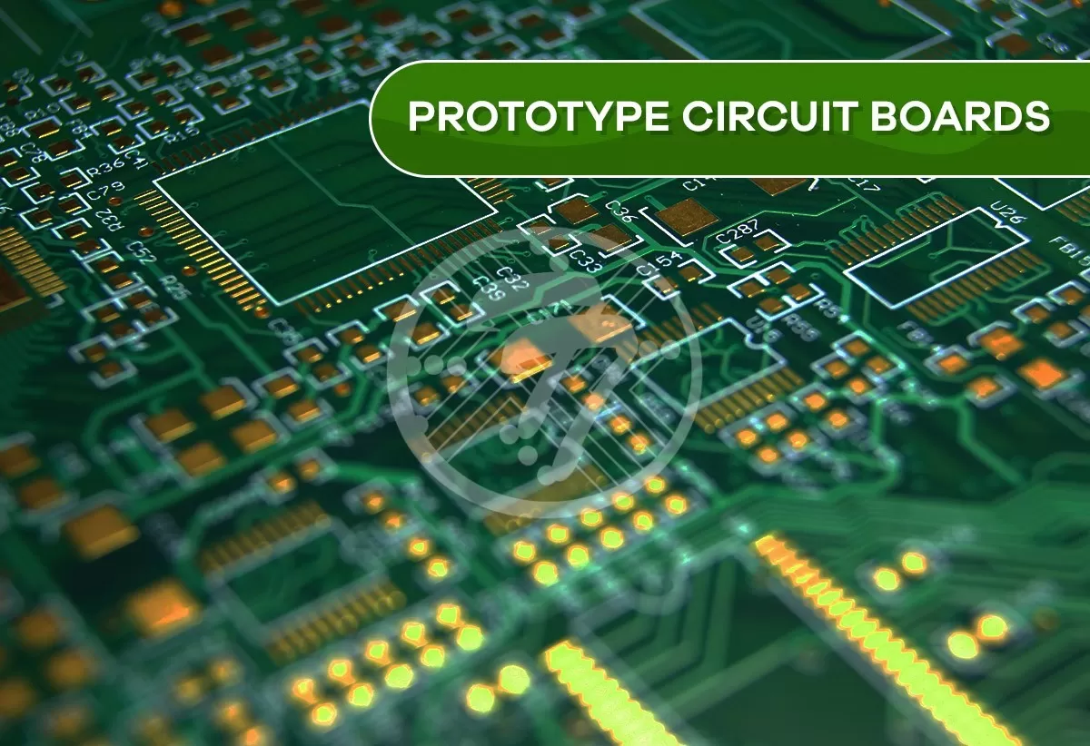
Prototype Circuit Boards with Surface Mount Components or Device

By | Date posted: | Last updated: February 14, 2022
prototype-circuit-boards

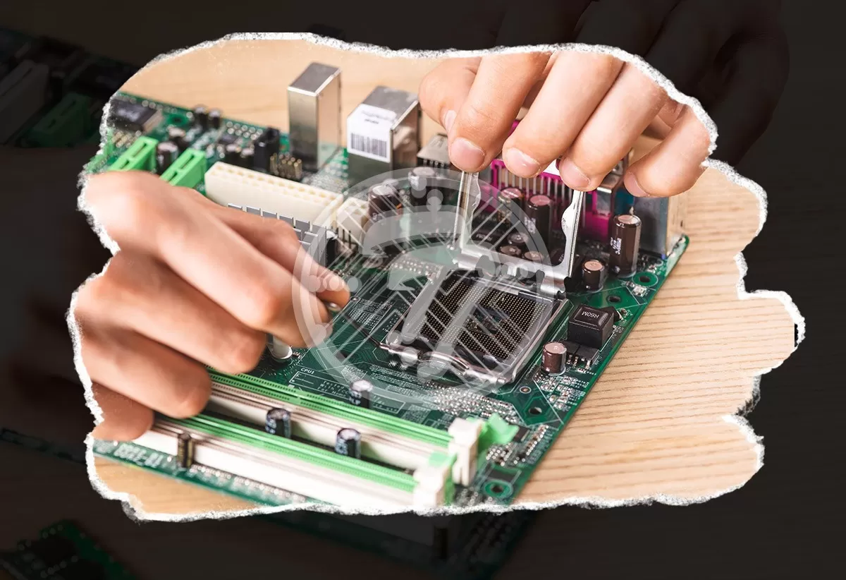
When manufacturing product, designing its prototype is very important. A prototype is a copy of the product being developed that gives a fair idea about how the device or product works or how it will look like. Engineers use prototype circuit boards for prototyping the electronic device. These circuit boards have small holes in which the electronic elements are fixed to get the required design. It is a common practice that many electronic engineers use prototype circuit boards with a surface mount component or device, but the question is: is it feasible? Let us delve into that.

What are surface mount devices, and how they are used with prototype circuit boards?

Surface mount technology is the prime method through which prototyping is done for electronic devices. The surface mount technology (SMT) is placed above the printed circuit board. Prototype Printed Circuit Boards Manufacturer use SMT technology only for making prototypes. The components are assembled in one place, and they are placed on the printed circuit board through the Solder-reflow process.

Specifications to be looked upon while making a Prototype Printed Circuit Boards with a surface mount component device?

Some things are required that has to be checked or looked upon while you are building a Printed circuit board-

1. Dimension

You must choose the right dimensions for your PCB. The measurements should be exactly that should take no extra space because the extra things left out are only waste material and can’t be used further.

2. Layers

It is good if the PCB has more layers, because more layers offer a better roadway to the electrical components making it more complex and unique.

3. Material

The best material for PCBs is copper, as there are a lot of benefits of using Heavy Copper in PCB Fabrication. Other than that, PEEK, Teflon, and Polyamide can also be used. The printed circuit board is typically made of glass- epoxy.

4. Board thickness

The more thickness the PCB has, the better it is, allowing a faster and inexpensive experience. The maximum thickness that is accurate is 1.5 mm.

5. Plating

Plating is an important component while designing a PCB when assembly and plating are done to cover the surface with another metallic material so that soldering can be improved.

6. Impedance control

This feature can become a problem for PCBs that have radios. The performance of the wireless antenna gets maximized if the impedance is controlled.

7. Minimum spacing and width

The PCB manufacturer decides the spacing and width. When we talk about the spacing, it refers to the copper width in the PCB.

8. Hole sizes

Big holes always remain a big no-no as they occupy more space and are very complex. Small holes are always preferred as it becomes easy to make electrical connections through it, and also, less space is needed.

9. Solder mask

The polymer is applied above the copper tracing to prevent any short circuits as the polymer is an insulator. The polymer acts as a solder mask.

10. Silkscreen

In silkscreen, graphics and texts are added to your printed circuit board.

Advantages of Prototype SMT Circuit Boards

  1. By using SMT technology, the size of the prototype will remain the same, just like the original piece. If the size is the same, you will get a better idea of the original product by looking at the prototype made with SMT technology.
  2. The minute and tiny size of SMT Assembly allows better flexibility because of the holes present. Also, the chances of parasitic attacks are less in these cases.
  3. This technology makes it easier to interchange the resistors and capacitors to try distinct values.
  4. This technology is cost-effective and a time saver.
  5. It gives fast results so that the product can be launched quickly in the market.
  6. The costs for modification of tools is also lower.

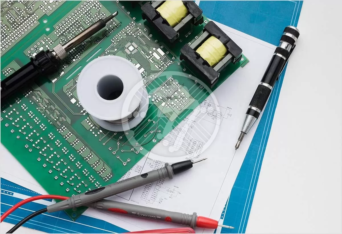
Process of assembly of Prototype SMT Circuit Boards

The assembly process of Prototype SMT Printed Circuit Boards is divided into three stages-

First stage

  • In the first stage, keep the printed circuit board on a rough surface, place the stencil above the PCB from the right side.
  • Keep on adjusting it till the perfect alignment is achieved.
  • Put solder paste on it.
  • Once the paste settles on it, detach the stencil carefully. Make sure there is no smudging.

Second stage

  • Place the other elements but make sure that you use the right parts and the orientation is also correct.
  • Ensure that the solder paste doesn’t get dried up completely.
  • Keep the PCB in the reflow oven and make sure it gets heater properly.

Third stage

  • After taking the PCB out of the oven, clean the PCB with a cleaning solution such as Isopropyl alcohol. Brush it properly.
  • Connect the PCB to power so that testing can be done beforehand.

Guidelines for Surface Mount Assembly & Prototyping

  1. A stencil that is unframed is always preferred as it comes at an affordable price. The framed stencils are comparatively expensive and difficult to deliver.
  2. Make sure that you handle the PCB with care because it is very delicate when it is made.
  3. Make sure you use superior quality lead paste for pasting.
  4. When you check the PCB working, make sure it passes the test 100%, else it won’t be passed forward.

Probable mistakes that can happen

  1. Design is the incorrect or wrong layout.
  2. sufficient attention is not given to the design’s testing, especially its probe points (access points).
  3. The elements or components are not used properly in the prototype according to the design.
  4. The parts that were used were not of superior quality.

These are important things for any Circuit Boards Prototyping to have with the use of surface mount devices. This is why we need prototype circuit boards with surface mount devices. The assembly process is quite simple: follow the steps carefully and don’t commit probable mistakes.

At Technotronix with our advanced engineering to deliver unparalleled quality and PCB Prototype services. With quick Printed Circuit Boards Prototyping and consistent delivery of high-quality PCBs, we offer a robust source of competitive advantage to our clients. With our four decades of experience, you can rest assured that we are cognizant of the industry best practices and will keep you ahead of the curve. We are providing high quality and defect free PCB Prototype as per customer specification. Get a Quick Quote for Prototype Circuit Boards.

How Rapid Prototyping PCB is Revolutionizing PCB Manufacturing in terms of Growth?

By | Date posted: | Last updated: September 21, 2021
Rapid Prototyping PCB

In a competitive scenario where go-to-market is an important aspect of product success, the role of speed cannot be overstated! In short, the less the time it takes for a company to move from concept to product stage, the more the scope of its success.

This is something that a rapid PCB prototype manufacturer can ensure. Before we delve into the how, it will be prudent to look at what really is the rapid PCB prototype process?

In short, Rapid Prototyping PCB process is a set of methods that you can use in order to create a prototype of your product. In turn, the prototype can then be used to validate your final product. The fact that variations of a prototype can be created in a short time span gives a significant boost to your product plans. The process of rapid prototype development rests on an additive manufacturing approach as opposed to a subtractive approach that involves frequent rework. Essentially, what the rapid prototyping approach rests on is 3D printing technology. This technology, in turn, involves creating a product replica by adding layers of material. The process begins with creating a computer-aided design file, that is popularly known as a CAD file. The file, in turn, is converted into a STL format which can be used for 3D printing and hence for rapid PCB prototyping. As opposed to this method, if the subtractive method is used, it takes more time, is wasteful and is also replete with hazards as it exposes the operator to hazardous chemicals.

Some of the features of 3D printing is as below:

  • Is quick
  • Ability to work with different materials
  • Low manufacturing cost
  • Lends itself to green manufacturing

Here is how the rapid PCB prototyping process is revolutionizing PCB manufacturing:

Testing of the product

First up, it allows for in-depth validation of the product and ensures you do not have to contend with costly mistakes when the full production batch is starting in your face. Rapid Prototyping of PCB allows you to detect any flaws early on and make necessary amends in time. That way your final product is far better whether you look at it in terms of functionality or aesthetics. Check out the guide to know why in-house Rapid PCB Prototyping crucial for innovating Product Development.

Cost Optimization

A major benefit of the technology is its cost-optimization. With 3D printers becoming far more affordable, its access isn’t just restricted to large businesses. In fact, rapid prototyping is a big boon for startups who are dealing with limited budgets and need to showcase a minimum viable product to potential investors. Also, with quick realization of your product concept, it also gives you the freedom to fail faster. You have the ability also to improve your product before it goes in for final production.

Acceleration of the PCB manufacturing process

While traditionally converting a concept into a finished product requires a lot of time and effort, with 3D printing, the process is significantly accelerated. It significantly cuts down the time required to create the prototype. For this reason, you can also make any changes in design easily. What it in essence does is to hasten the final manufacturing process.

To say, therefore, that the PCB manufacturing process has been revolutionized, therefore, isn’t an overstatement. Not only does it save time, importantly it prevents you from any rude shocks at a later time. With a prototype in hand, you can get a reliable validation of your product or insights into any changes required, as the case may be.

At Technotronix, we are equipped with state-of-the art technology to cater Rapid PCB Prototype requirement. Also importantly our team of experts can offer you great insight into industry best practices so that costly mistakes are avoided. The fact that we have over 40 years of experience in fabricating prototypes as well as full production runs, ensures that you can rely on our capabilities. With the ability to offer turnkey services, you can count on us for your requirements. The added advantage with us is that we are committed to quick turnaround times, which help you see results quickly. A wide range of clients, across industries, stand as a strong testimony to our success.

Get in touch with us for high quality and defect free rapid PCB prototyping as per customer specification. Visit us to know more about our PCB prototyping services and feel free to contact us.

How to Choose the best PCB Prototype Service for Your New Product Introduction (NPI)?

By | Date posted: | Last updated: September 5, 2024
PCB Prototype Service

When it comes to electronic devices, it is an ever-growing industry with new devices hitting the market every single day. The process of a new launch, however, is quite complex. You need to go through the entire development cycle and that too in the shortest possible timeframe. The one thing that is invaluable in this phase is PCB prototype service. With a successful prototype you tend to reap many advantages including but not limited to the fact that there isn’t the fear of costly mistakes later.

With a number of contract manufacturers offering PCB Prototype services, how exactly does one choose the right partner who will be extremely crucial to the success of your final product. Here is a handy guide:

Quality of the PCB Prototypes

This of course, is the most important aspect of the choice. You want the prototype to be free of any errors, the material to be defect free and more. In order to assess the kind of quality offered by the PCB Prototype manufacturer, you need to run through the following aspects:

  • Availability of state-of-the-art equipment
  • Quality of expertise available
  • Client portfolio and testimonials
  • What kind of focus do they have on prototype fabrication

It will also help to check what kind of experience the PCB prototyping USA, service has in your particular industry. With a service that has a great track record in your industry, what you will have access to is a whole body of industry insights that will come in extremely handy. Simply put, you will not be required to reinvent the wheel.

Minimum Order Quantity of PCB Prototype

This is a very important aspect of choosing your PCB service. After all, a prototype does not allow you give the assurance of a high order quantity. A manufacturer who has a prototype focus, will not, therefore insist on a high quantity that does not meet your requirements.

Turnaround Time of PCB Prototype

When you are dealing with a new product introduction (NPI) or if you are a startup wanting to showcase a minimum viable product to an investor, time is of essence. You clearly need a PCB prototyping service that understands this aspect and offers quick turnaround time. There is no way you want to sacrifice on quick delivery, ensure therefore that you check the delivery schedule of the manufacturer. It will also be prudent to reach out to existing clients to see what their experiences related to deadlines, have been.

Bespoke products

You would want to go ahead with a PCB prototype USA, service, that customizes the prototype to your bespoke requirements. This would be in terms of size, shape, components, bespoke surface finishes and more. For this the PCB service will have to be armed with the right tools as also people who have the right expertise in dealing with it.

Packing & Shipping

Ever so often it may not strike you to check whether the PCB prototype service offers packaging and shipping services. However, this is also an important aspect to check for, so that you can rest assured that the products can be safely delivered.

PCB Prototype Cost

Last, but certainly not the least, what you need to check for, is the cost. The price of the PCB certainly goes on to impact the final cost of your product. For this, it is important that the manufacturer can offer you quick quotes that in turn help you price the product.

While optimal pricing is key, you need to also remember that you cannot sacrifice quality at the altar of price. You do not want a situation where you have gone with the lowest cost offered and in the process have had to redo the entire process as quality was sacrificed. A proven PCB prototype service with years of experience in the field is really your best bet in receiving quality products that do justice to your electronic device.

Also checkout: How much does a PCB prototype Cost?

Overall, it is important to remember that any lapse or wrong decision made in choosing the PCB manufacturer can cost you dearly, in terms of time and monetary cost. Worse still, a poor-quality PCB and hence a poor electronic product, can cost you hard-earned company reputation.

At Technotronix, we combine state-of-the-art technology with our advanced engineering to deliver unparalleled quality and service. With quick PCB prototyping and consistent delivery of high-quality PCBs, we offer a robust source of competitive advantage to our clients. With our four decades of experience, you can rest assured that we are cognizant of the industry best practices and will keep you ahead of the curve. We are providing high quality and defect free PCB Prototype as per customer specification. Visit to know more about PCB prototyping services and feel free to contact us. Also, you can drop an email to us at [email protected].

Why you need to Optimize Bill of Materials for Rapid PCB Prototyping?

By | Date posted: | Last updated: September 5, 2024
Rapid PCB Prototyping

If there is a buzzword when it comes to new product development, it has to be Rapid PCB Prototype. The need to get your product to market in the shortest possible time is pressing, if you need to maintain a competitive advantage. With several stakeholders- manufacturers, suppliers, engineers, designers involved in creating the end product, the one thing that is needed is that everyone speaks the same language. It is only when there is consistency in communication, can the end result be of high quality. This will also ensure that there is no time wasted in to and fro communication, leading to delays.

Effectively, when it comes to Bill of Materials, ensure that your prototyping is indeed “rapid”.

To optimize Bill of Materials for Rapid PCB Prototyping consider following list:

Effectively, what this means is optimizing the Bill of Materials for rapid PCB prototyping. Here is a list of things that you need to follow when it comes to your BOM, to ensure that your prototyping is indeed “rapid”.

Exhaustive and detailed

The thumb rule to follow when it comes to the BOM is to be as exhaustive and detailed as possible. It is always better to over-communicate as opposed to leaving some details ambiguous and therefore open to assumptions and interpretations. Including the minutest details such as the maximum voltage on your capacitors will go a long way in ensuring there is no element of doubt. This way, the manufacturer will be totally up-to-speed on your exact requirements and is likely to deliver the PCB prototype as per your expectations.

Labeling

Now this is another very important aspect of the Bill of Materials. There could be some parts that are absolutely critical to your design, where you will have the exact part number mentioned. However, there could be some parts where you are fine with using any substitute as long as it caters to the broad specifications. There could be some other parts where you would be open to substitutes but would want to approve them before they are implemented. It is absolutely imperative to specify this as far as your labeling goes. By marking this on your BOM or color-coding it, you are ensuring that you get exactly what you want.

Keep a tab on changes

With the BOM being referred to by multiple stakeholders and changes being made to it, it is crucial to keep a tab on these changes. In the absence of a tracking mechanism you will be left wondering why particular changes were made and the kind of implications they may have. What is needed, therefore, is a mechanism whereby changes are tracked. You could have different version documents or revision histories to keep everyone up-to-speed. The efficiency it will bring about cannot be overstated.

What you also have is great documentation, should you want to revise the product at a later date.

Following the above best practices will bring about the following advantages:

The product will be accurate

This is the biggest advantage of optimizing your Bill of Materials; you will get an accurate product. There will, therefore, be no need to correct costly mistakes at a later stage. The BOM will serve as a perfect how-to-guide and bring about a final product that meets your bespoke requirements. Check out the guide on Why Bill of Materials (BOM) is important in PCB Manufacturing process.

What you will also have is a scenario where wastage and errors are avoided. This means optimizing your costs and having a cost-effective product.

Speaking of costs, what the BOM additionally does, is to help you correctly predict the cost of the prototype. With each part listed and specifications mentioned, it is fairly easy for you to determine the exact cost. What you have, therefore is no fear of surprises sprung at you at a later date.

Adherence to timelines

This is the “rapid” bit in the rapid prototyping. With exact specifics of each part and exhaustive communication, what you have is no time wasted on back and forth communication and therefore strict adherence to timelines

To sum up

Once you have a great idea, an imperative step in its execution is to have a robust Bill of Materials in place. With an exhaustive BOM, what you have is not just a document, but a fool-proof method of avoiding errors and misunderstandings that can prove to be costly. With a detailed Bill of Material, you can rest assured that what will get is your desired product, within the timelines that you need it.

We providing high quality and defect free PCB prototyping and assembly as per customer specification. Visit us to know more about our PCB prototyping services and feel free to contact us. Also, you can drop an email to us at [email protected].