How Medical PCB Prototype Plays a Major Role in Modern Medicine & Its Emergence!


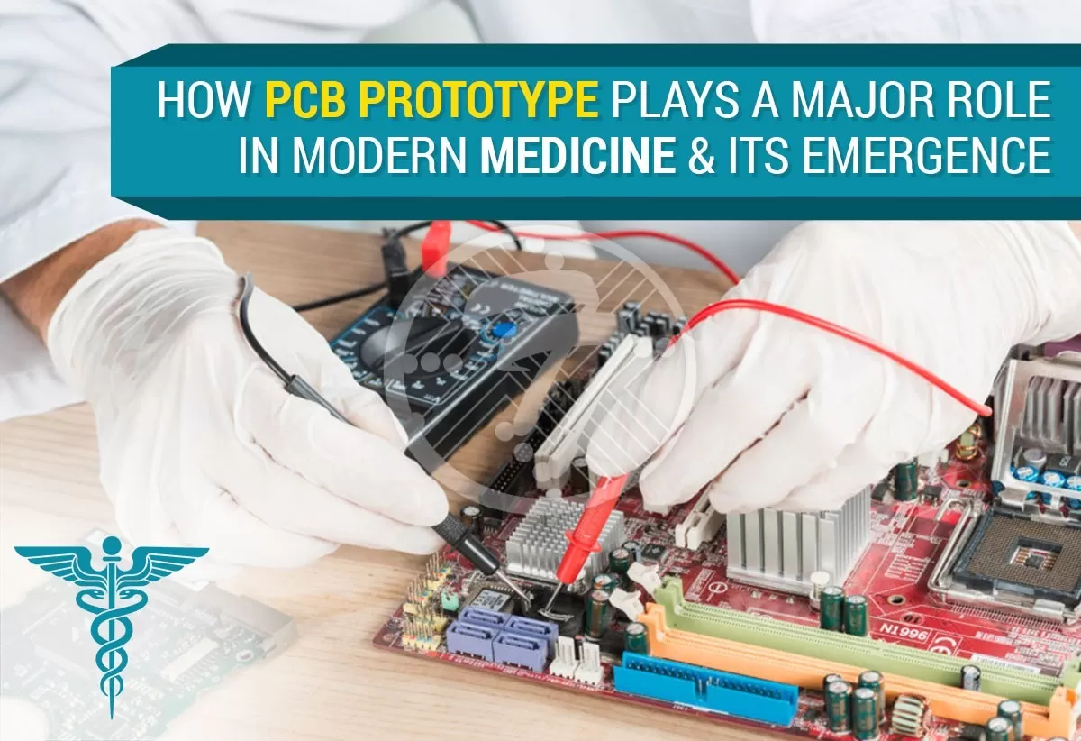
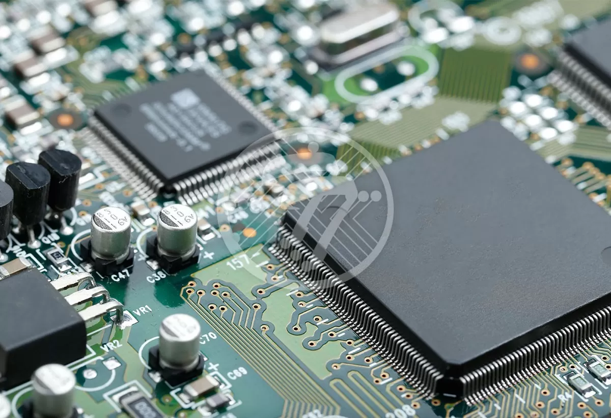
As with many other industries, PCBs play a critical role in medicine and healthcare. From being used in pacemakers, medical imaging applications, body monitoring devices and more, their use is quite ubiquitous. Here is a broad overview of the role played by PCB prototypes in different aspects of modern medicine:
Implantable Medical Devices
These include a range of devices such as:
- Cochlear implants for the hearing impaired
- Implanted defibrillators for those who are at an elevated risk for cardiac issues
- Responsive Neurostimulators for those dealing with epilepsy.
In each of these cases, basis the bespoke requirements of the patients as well as the needs of the implant, PCB prototyping can be undertaken.
Medical PCB Prototypes in Imaging
Medical PCB Prototypes have a huge role to play in the field of medical imaging.
Once again PCBs are used in a wide range of medical imaging devices such as:
- MRIs
- CTs
- Ultrasound equipment
Monitoring Medical PCB device
PCB technology also finds wide application in monitoring devices such as:
Temperature monitors
Blood glucose monitors
Blood pressure monitors
- Temperature monitors
- Blood glucose monitors
- Blood pressure monitors
Some of the other devices that also make use of PCB Prototyping service include:
- Pacemakers
- EMG systems
- Peristaltic infusion technology
- Muscle stimulation equipment and more
In each of the cases the PCBs need to be created to cater to the specific requirements or lab settings, as the case may be.
What works well for medical devices?
When it comes to medical devices, Surface Mount Technology Assembly works best.
The big advantages with SMT when it comes to PCB Prototyping include the following:
- It allows for ease of automation as opposed to the through-hole method
- It is far less expensive than the through-hole method
- It takes up less space and is therefore extremely useful in the world of miniaturization
- With most medical devices required to have constant motion, SMT is a better fit.
Requirements for Medical Device Manufacturers
When it comes to medical device manufacturers, two important aspects need to be kept in mind. The first are to do with the design and the other of course to do with complying with the necessary FDA guidelines.
To arrive at an optimal design, some of the questions to answer, include:
- What is the purpose of the device
- Can it be reduced in size without affecting its functionality?
- Is it flexible?
With flexible and rigid-flex PCBs available these days, there is enough and more possibility to keep the devices as flexible as possible.
The next set of guidelines to follow, are to do with the FDA regulations. Some of these include:
- Registering your establishment with FDA
- Listing your device with FDA
- Adhering to Quality System regulations, and more
Why you can choose TechnoTronix for Medical PCB Prototyping Service?
Choosing your electronics assembly partner is crucial for any business, as it is the PCB that can make or mar the performance of any electronic product. However when it comes to medical devices, the importance of reliable PCBs increase many fold. It is therefore imperative that the partner be chosen with extreme care.
At Technotronix, we have over four decades of experience in rendering PCB Assembly and manufacturing services. We adopt advance production techniques and manufacturing practices that result in multi-layered PCBs with bespoke layouts. Our competitive edge comes from the fact that we can offer fast prototyping and consistent, on-time delivery of quality products.
The fact that we are extremely conversant with the fact that the medical PCB prototyping industry requires high degree of innovation, means that we can partner with you effectively to take your healthcare solutions to the next level. Our quick turnaround times and the fact that we are an ISO 9001:2015 AS9100 Rev D company with an unrelenting focus on quality means that you can rely on us for your medical PCB Prototyping needs.
At TechnoTronix, when designing a medical device PCB prototype, we especially keep the following issues in mind:
- We design boards so that it is easy to test and debug
- The boards are designed for ease of assembly and serviceability.
In addition, our Medical PCB Prototypes adhere to the following:
- Reduced timelines
- Accurate, reliable prototypes
- Reduced costs
- Efficient project completion
At Technotronix, we combine state-of-the-art technology with our advanced engineering to deliver unparalleled quality and service. With fast PCB prototyping and consistent delivery of high-quality PCBs, we offer a robust source of competitive advantage to our clients. With our four decades of experience, you can rest assured that we are cognizant of the industry’s best practices and will keep you ahead of the curve. Visit to know more about PCB prototyping service and feel free to contact us. Also, you can drop an email to us at sales@technotronix.us.